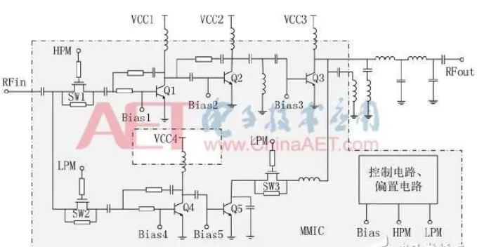
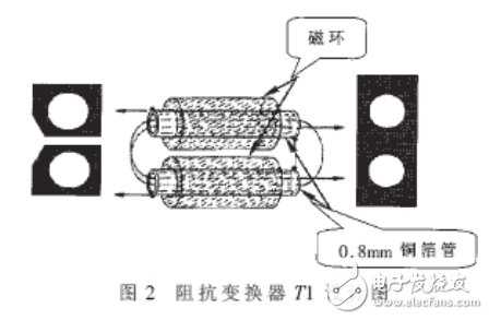
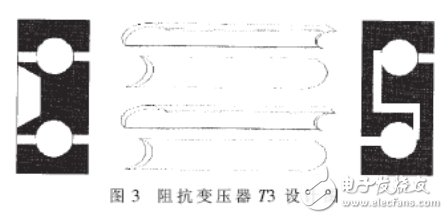
Pulse power amplifier design Assembly and commissioning of pulsed power amplifiers Circuit design Circuit board (PCB) and transmission line transformer design Thermal design The high-power wide-band linear RF amplifier module is widely used in important communication systems such as electronic countermeasures, radar, and detection. Its broadband and high-power generation technology is a very key technology in wireless electronic communication systems. With the development of modern wireless communication technology, broadband high-power technology, wide-band frequency hopping, and spread spectrum technology have placed higher demands on the design of solid-state linear power amplifiers, that is, the frequency of the RF power amplifier is widened, and the output power is larger. The overall equipment is modular. Generally, broadband RF power amplifiers designed in the HF~VHF band use FET design rather than simple power transistors. It is based on the high input impedance of the FET and the relative impedance of the input impedance. The change does not have too much deviation, easy impedance matching, and the bias circuit is relatively simple, and the designed amplifying circuit has high gain and good linearity. The high-power wide-band linear RF amplifier of this paper is designed by MOS field effect transistor (MOSFET). It adopts class AB push-pull power amplification mode. Its working frequency range is 0.6M~10MHz, and the output pulse power is 1200W. After debugging, the amplifier works stably and has reliable performance. Test instruments used for commissioning, testing, and utility include oscilloscopes, spectrum analyzers, power meters, high-power coaxial attenuators, network analyzers, and RF signal generators. Circuit design The designed broadband high-power pulse amplifier module requires a working frequency band greater than 4 octaves, and the output power is large, which has high suppression of harmonics and clutter. In addition, since the harmonics are in the operating frequency band, an amplifier is required. The module has a high degree of linearity. For the design requirements, the RF power amplifier amplification chain in the design uses a three-stage FET, all of which use MOSFETs. Each stage of amplification uses Class AB power amplification mode, and both use push-pull mode to ensure that the power amplifier module can work in broadband. Considering that it is convenient to use a positive voltage for the power supply, an enhanced MOS FET is used. In addition, in order to broaden the frequency band and output high power, transmission line broadband matching technology and feedback circuit are adopted to meet the design requirements. Since the output requirement of the RF power amplifier is high-power pulsed emission, it is required that the MOSFETs used in the first and second stages should have fast switching to ensure that the falling edge and the rising edge of the pulse modulation signal are intact, and the clutter and harmonics are reduced. interference. The first and second stage power amplifiers in the design use MOSFETs as IRF510 and IRF530. The final stage power amplifier requires an output pulse power of 1200W. To avoid using power synthesis techniques, MOSFET MRF157 is selected as the final power output stage. The schematic diagram of the designed RF pulse power amplifier circuit is shown in Figure 1. The transmission channel is established after the signal source generates the RF signal and then passes through several stages of intermediate stage amplification to input the signal to the power amplification stage, and finally the RF signal is transmitted through the antenna. In Figure 1, the input signal is 20~21dBm, 50Ω input; the working voltage is 15V and 48V, of which 15V provides working voltage for the first and second power amplifiers, 48V provides working voltage for the last stage power amplifier; 6V regulated output can be used 15V or 48V for voltage regulation conversion, the overall design of the circuit uses Class AB power amplification, the design of the standing wave ratio is 1.9. The signal amplified by the intermediate stage is first converted into a power amplifier by T1 (4:1) impedance transformation. In the upper half of the signal, Q1 is turned on, and the second half of the signal is turned on. Q2 is turned on. Then, the T2 (16:1) impedance transform is used to enter the second stage of amplification. The upper half of the same period Q3 is turned on, and the lower half of the period is Q4. Turn on, complete the energy amplification of the entire signal cycle; use the T3 (4:1) impedance conversion to enter the final stage of amplification to continue to increase the operating current to drive the high power MOSFET MRF157. To ensure a 50Ω output, the impedance at the output is converted to T4 (1:9). The purpose of using a negative feedback circuit in the circuit is to generate a relatively stable power gain over the entire bandwidth frequency response, maintain the linearity of the gain, and introduce a negative feedback circuit, which is beneficial to improve the stability of the input return loss and the low-frequency end signal power amplification. . In addition, in each stage of the circuit design, a sliding varistor is used to set the bias voltage of each tube, which greatly reduces the occurrence of crossover distortion, and makes the waveform of the amplified signal in the upper and lower half cycles as much as possible. b. Circuit board (PCB) and transmission line transformer design In order to ensure the consistency of signal amplification in the entire frequency band and reduce the influence of clutter and harmonics, the broadband high-power RF amplifier adopts class AB power amplification to ensure the symmetry of the circuit. When designing the PCB, try to ensure that the copper film traces are symmetrical and of the same length. In order to facilitate the selection of the dielectric constant of the PCB, the entire PCB board is a lead tin plate. The Smith chart software was used at the signal input and output to calculate and simulate the shape and size of the copper traces to ensure a good match of impedance characteristics. One of the key technologies in the design is the design and fabrication of transmission line transformers. The transmission line impedance converter can be used to achieve impedance matching between the signal source and the input or output of the power MOSFET, maximizing the bandwidth potential of the tube itself. Transmission line transformers must have two points in design and use: first, the matching relationship between source impedance, load impedance and transmission line impedance; second, the input and output terminals must meet the specified connection and grounding methods. Since the class AB power amplification method is adopted in the design, the input of the primary coil and the output of the secondary coil should be as symmetrical as possible. A total of four transmission line transformers T1, T2, T3 and T4 are used in the design. In the first two stages of power amplification, the secondary coils of T1 and T2 are one turn, and the secondary coil of T3 is two turns. This is because the saturation of the magnetic material often occurs at the low frequency end, increasing the primary and secondary coils of T3. The number is beneficial to improve the performance of the low frequency end. T1, T2, and T3 use the core of the coaxial line SFF-1.5-1 as the primary coil transmission line, and the secondary coil is made of a copper foil material, and a copper foil having a thickness of 0.8 mm is used. The T4 is an imported high-power transmission line transformer (model: RF2067-3R). The designed T1 is shown in Figure 2. The dark areas in Figure 2 represent the copper area. The copper foil tube first passes through the magnetic ring and then passes through the copper sheets at both ends and is welded together to complete the secondary coil. The design of the T2 is basically similar to that of the T1, except that the number of turns of the primary coil wound by the core of the coaxial line SFF-1.5-1 is different. The production of the T3 secondary coil has changed somewhat in order to enhance the passage of low frequency signals. The copper foil tube is not used, but the copper foil is bent into an arc shape. As shown in Figure 3. Two copper foil pieces are passed through each of the magnetic ring holes, and are respectively welded to the copper film plates at both ends, so that the secondary coil of the entire coil is two turns, and then the winding of the primary coil is completed according to the impedance ratio. The purpose of this is to increase the number of turns in the primary and secondary at a fixed impedance ratio to improve the low frequency characteristics of the amplifier. c. Heat dissipation design For RF power amplification, the output power is large, the power consumption of the tube is also large, and the heat generation is very high, so the heat must be dissipated to the tube. According to the power consumption PD of each stage tube and the thermal characteristics of the tube, these thermal indexes include the thermal resistance RθJC of the device die transmitted to the device case, the allowable junction temperature of the device is TJ, and the working ambient temperature is TA, etc., which can be calculated. The size and type of heat sink material that needs to be used. In this design, the operating temperature of the device is 55 ° C, the aluminum heat sink size is 290mm & TImes; 110mm & TImes; 35mm, and the DC fan is required to heat the last MOSFET. The amplifier tubes used in the design are all MOSFETs. Due to their very poor antistatic performance, the tube will be burned out due to static electricity on the soldering equipment, especially the last stage of high power MOSFET (MRF157). Be especially careful. Before designing the circuit, you can use the device model in MulTIsim software or Pspice software to familiarize yourself with the use of IRF510 and IRF530. When the circuit starts to debug, the bias voltage setting of the last stage MOSFET MRF157 can be omitted. First, the static working point of MRF157 is set by the amplification effect of the first two stages of the test. The first two stages of the signal amplification result obtained by the test are about 100V Vp-p (high resistance input). The operating point voltage of each tube should not be too high during commissioning, which is slightly higher than the opening voltage VGS(TH). Always monitor the operating current at the power supply to prevent excessive current. Adjust the static operating point by fine-tuning the transformer at the gate end of each tube to minimize waveform distortion. The oscilloscope can now be used to monitor the waveform output. According to the actual results of the first two stages of circuit debugging, the first stage mainly affects the amplified amplitude, while the second stage affects the amplified waveform. When commissioning the last stage of power amplification, MRF157 must be very cautious because it is too expensive. For each debugging, set the static working voltage of each tube as much as possible, and do not change the static working point dynamically. The terminal is connected to the spectrum analyzer after being connected to a 50Ω high-power coaxial attenuator. The output power, as well as the harmonic components, can be obtained from the frequency domain waveform of the spectrum analyzer. The wideband high power amplifier designed in this paper was assembled and tested in a laboratory environment and tested with the transmitting coil for a long time. The test and practical application show that the amplifier operates normally and works reliably. It can complete the high-power amplification of broadband RF pulses, meets the design requirements, and plays a great role in a certain detection device working in this frequency band with good effect. The utility model provides a disposable electronic cigarette, comprising: a hollow shell, the bottom of the shell is provided with a lower cover; the shell contains an atomizer, and the outer side of the atomizer is sheathed with a disposable cigarette A bomb, a microphone cover is arranged under the atomizer, a microphone is covered under the microphone cover, a battery is arranged on one side of the atomizer, and an upper cover is arranged on the top of the casing; The atomizer includes an atomizing core, an oil-absorbing cotton sleeved on the outside of the atomizing core, and an atomizer outer tube sleeved on the outside of the oil-absorbing cotton. The disposable electronic cigarette provided by the utility model absorbs the smoke oil on the surface through the absorbing cotton, and then atomizes the smoke through the atomizing core, which greatly reduces the risk of oil leakage, at the same time, reduces the burning of cotton and ensures the smoking taste.The utility model provides a disposable electronic cigarette, comprising: a hollow shell, the bottom of the shell is provided with a lower cover; the shell contains an atomizer, and the outer side of the atomizer is sheathed with a disposable cigarette A bomb, a microphone cover is arranged under the atomizer, a microphone is covered under the microphone cover, a battery is arranged on one side of the atomizer, and an upper cover is arranged on the top of the casing; The atomizer includes an atomizing core, an oil-absorbing cotton sleeved on the outside of the atomizing core, and an atomizer outer tube sleeved on the outside of the oil-absorbing cotton. The disposable electronic cigarette provided by the utility model absorbs the smoke oil on the surface through the absorbing cotton, and then atomizes the smoke through the atomizing core, which greatly reduces the risk of oil leakage, at the same time, reduces the burning of cotton and ensures the smoking taste.The utility model provides a disposable electronic cigarette, comprising: a hollow shell, the bottom of the shell is provided with a lower cover; the shell contains an atomizer, and the outer side of the atomizer is sheathed with a disposable cigarette A bomb, a microphone cover is arranged under the atomizer, a microphone is covered under the microphone cover, a battery is arranged on one side of the atomizer, and an upper cover is arranged on the top of the casing; The atomizer includes an atomizing core, an oil-absorbing cotton sleeved on the outside of the atomizing core, and an atomizer outer tube sleeved on the outside of the oil-absorbing cotton. The disposable electronic cigarette provided by the utility model absorbs the smoke oil on the surface through the absorbing cotton, and then atomizes the smoke through the atomizing core, which greatly reduces the risk of oil leakage, at the same time, reduces the burning of cotton and ensures the smoking taste. maskking vape,maskking vape price,maskking vape review,maskking vape shop,,maskking vape cost,maskking vape disposable,maskking vape informacion Suizhou simi intelligent technology development co., LTD , https://www.msmvape.com
Figure 1 

Dry goods! Design and Analysis of High Power Broadband RF Pulse Power Amplifier
Center topic: