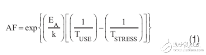
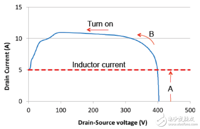
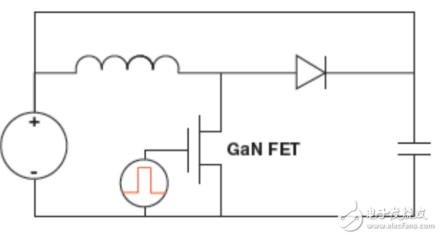
TI is designing a comprehensive quality assurance program based on the GaN principle and related application testing to provide a reliable GaN solution. The material properties of gallium nitride (GaN) make the power switch an exciting and groundbreaking new feature – power GaN. High Electron Transfer Transistor (HEMT). The HEMT is a field effect transistor (FET) that makes the on-resistance much lower. Its switching frequency is faster than the equivalent size of silicon power transistors. These advantages make power conversion more energy efficient and enable more efficient use of space. GaN can be mounted on a silicon substrate to take full advantage of silicon manufacturing capabilities and achieve lower cost. However, when using new technologies, it is necessary to verify the reliability of this technology. The subject of this white paper is precisely the characterization of GaN devices. Introduction With more than 30 years of experience and continuous improvement, the industry takes it for granted that silicon power transistors are highly stable. This long-term user experience has formed a mature system of quality identification methods; in this system, reliability and quality are certified by running standardized tests. These tests are based on in-depth studies of fault mode understanding, excitation energy, and acceleration factors, as well as the development of statistical and mathematical frameworks for estimating lifetime, failure rate, and defect rate. This quality identification method system has now proven to be effective and practical because several generations of silicon products can be operated under real service conditions for real life. However, GaN transistors are recently developed devices. RF GaN HEMTs on more expensive silicon carbide substrates have been widely used in wireless base stations, and their reliability has been verified [1]. Although based on similar basic principles, power GaN HEMTs add more features in achieving higher voltage processing. It is rooted on a silicon substrate and uses materials compatible with silicon manufacturing to reduce costs. In addition, for fail-safe reasons, it needs to be an enhanced mode (e-mode) or a normally closed device. There are three main architectures: 1. Depletion mode (d-mode) insulated gate GaN HEMT with an e-mode Si FET; 2. e-mode insulated gate GaN HEMT; 3. P-type e-mode junction gate GaN HEMT. These three devices have different failure modes for their own reasons and the effects of silicon FETs. The question is how to identify their quality. The silicon-based standard quality identification method is a valuable and landmark method for quality and reliability identification, but it is unclear how it works for GaN transistors in terms of device lifetime, failure rate, and application dependencies. Texas Instruments (TI) is an industry leader in semiconductor technology with long-standing experience in bringing reliable semiconductor products to market, including non-silicon material technologies such as ferroelectric random access memory (FRAM). We have great advantages in bringing reliable GaN products to market through GaN-related quality identification method systems and application-related tests. Standard quality identification method system In the identification of silicon power device quality, two standardization organizations' quality identification method systems have been widely used: Joint Electronic Equipment Engineering Committee (JEDEC); and Automotive Electronics Association (AEC) [2, 3, 4, 5]. These standards specify a number of tests that can be divided into three categories: electrostatic discharge (ESD), packaging, and devices. Electrostatic discharge requirements are a mandatory operating standard, so ESD standards are unlikely to change. Package testing is similar to those already done for silicon chips, and the root cause of the failure needs to be identified to emphasize the unexpected failure mechanism. The back-end processing previously used in silicon chips is also used for GaN. In this context, the similarities are highlighted because of problems such as package stress and bonding surface interaction. However, this device category is brand new and therefore of particular importance. The following paragraphs examine the standard silicon chip quality identification method system and describe how this method system can be applied to GaN. For silicon chip quality identification, the run time under standard stress is 1000h and the junction temperature is at least 125°C. Assuming an activation energy of 0.7 eV, the specified temperature acceleration factor is 78.6 [2]. This results in a stress at 1000 h of operating temperature at a junction temperature of 125 ° C equal to the stress experienced during the 9-year operating period at Tj = 55 °C. The devices are mass calibrated at their maximum operating voltage. For discrete power FETs, this is typically chosen to be 80% of the minimum breakdown voltage specification. This means that there is no built-in voltage acceleration under the qualification test conditions; voltage acceleration is only achieved by temperature. Since Tj is above 55 ° C, typically above 75 ° C, this can have a huge impact on power devices. This standard also specifies three batches of products, each with 77 components and should not fail under stress. The zero failure criterion in the 231 components means that the intra-batch defect allowable percentage (LTPD) has a value of 1 [2]. This means that you have a 90% confidence that 1% of the parts in a batch are defective under the presumed stress conditions. In other words, it is operated for 9 years at a temperature of Tj = 55 ° C and is biased at the maximum operating voltage. The initial maximum failure rate (FIT) is approximately 50. The FIT at Tj = 55 °C also uses an activation energy of 0.7 eV, derived from the zero failure results of 231 components. However, in addition to static testing, there is a dynamic test. It is very broadly defined as "a device that is likely to operate in a dynamic mode of operation" [3]. The test is defined by the manufacturer. The lack of specified tests is difficult because it is difficult to specify a test that corresponds to a wide range of evolving applications and technologies. The specified test may not be properly associated with the actual use environment, and may have an error failure or accelerate the effective failure mechanism [7]. For silicon FETs, the credibility of the quality identification method system has been established over many years of practical use. Unlike new technologies such as GaN, device vendors are responsible for determining that their dynamic tests can predict the actual operating conditions. Therefore, application-related stress tests need to be developed to verify reliability under actual use conditions. Finally, it is important to note that GaN cannot withstand avalanche energy. That is, the device will be damaged when it is broken down. This is a problem that needs to be addressed, especially for high voltage applications such as power factor correction (PFC) circuits; in these applications, the device is subject to possible overvoltage events, such as on power lines. Lightning spike discharge. Applicability of the standard quality identification method system Both JEDEC and AEC standards are based on sound fundamentals, but they are technically backward. Although the quality certification of silicon products is a valuable and milestone event, users need a continuous operation with low failure rate under the actual service conditions and within the required service life, say 10 years. product. Therefore, companies that introduce new technologies such as FRAM, proportional CMOS, and GaN need to understand the basic principles of these standards. In the JEDEC quality identification method system, the main contributing factor is temperature. The acceleration factor (AF) is calculated according to equation eq. (1), where EA is the activation energy and k is the Boltzmann constant. If eq (1) is used with a stress temperature Tj = 125 ° C, a temperature Tj = 55 ° C, and an excitation energy of approximately 0.7 eV, the resulting acceleration factor will be 78.6. This is also the reason why the 1000h stress at Tj = 125°C is roughly equivalent to 10 years when Tj = 55°C. In the published literature, the excitation energy [8] of GaN varies between 1.05 and 2.5 eV. These wide range of values ​​show the differences between devices, processes and materials in different laboratories and companies around the world. This range provides a greatly variable acceleration factor, such as 687 at EA = 1.05eV and a value above 5 million at EA = 2.5eV. Therefore, it is necessary to determine the excitation energy associated with the process and the device architecture of the final product. It is also important to take into account the junction temperature in actual operation. Due to its wide band gap, GaN can operate in higher temperature environments than silicon materials. This is important for power electronics. Table 1 compares the 1000 h silicon specifications at 125 ° C stress temperature with several other cases. As can be seen from Table 1, if a junction operating temperature of 105 ° C is required, the activation energy is assumed to be 0.7 eV, and the non-acceleration time is reduced from 9 years to 0.3 years. By increasing the stress temperature to 150 ° C (this is a practical limit for standard packages), it is possible to increase this time to 1.1 years. In this case, the stress test does not meet the equivalent lifetime of the field, or the maximum FIT rate condition of approximately 50 FIT is calculated. However, it is indeed a reliable and high quality milestone test method. A 1000 h stress test representing a 10-year usage time requires an acceleration factor of 87.6 and is achieved at an excitation energy of 1.37. Lower excitation energies such as 1.05 eV in Ref. [8] will require 2.84 times the voltage acceleration, or approximately a 6 to 17 week duration. Excessive voltage acceleration results in an unrepresentative failure mode, and duration extensions extend the development time of new products. Depending on the failure mode and the acceleration available in the package, a qualification test that represents the equivalent lifetime of the field may not be achieved. Lifetime requirements are guaranteed by wafer level reliability testing and verified by extended duration stress testing of packaged components. Table 1: Effect of different stress parameters on reliability and quality speculation data It is important to set the fault criteria based on the specific failure mode of GaN. A special fault is the increase in dynamic Rds on-resistance, also known as current collapse. This failure is caused by buffering and negative charge trapping on the top layer [9, 10]. The charge is trapped when high voltage is applied and does not dissipate immediately when the device is turned on. The trapped negative charge repels electrons from the channel layer, and the Rds on-resistance increases due to the decrease in the number of electrons in the channel layer (Figure 1). Subsequently, the Rds on-resistance is restored as the trapped charge is dissipated. This effect reduces efficiency and can cause the device to heat up too much and fail prematurely. Figure 1: The circuit cross section of a GaN device shows how the trapped electrons increase the Rds on-resistance by reducing the number of electrons in the channel layer. In addition, the trap density increases as the device ages, making the effects of dynamic Rds on-resistance more severe. We have dedicated hardware to monitor the dynamic Rds on-resistance during stress testing, which allows us to ensure that the released product does not have this problem. Application related test Although the DC test method is relatively simple when testing a large number of components, they may not predict whether GaN will have a 10-year lifetime in practical applications. Hard switching stress is different from DC stress. Hard-switching power converters have an inductive switching transition during which the device is simultaneously affected by high currents and high voltages. Since the FET channel requires a drain voltage, Vds, sinks the entire inductor current before falling, and reverse recovery discharges to other devices on that node, turn-on switching is the most stress-intensive process. It also needs to carry the device discharge output and the extra current in the switch node capacitor as Vds falls. Since the FET channel is closed when Vds is low and the inductor current is charged for the respective capacitor, the off stress is relatively low. The device stress is shown by a boost converter using the topology shown in Figure 2. Figure 3 shows the simulation results of the hard-switch-on transition on the primary-side switch (FET1). The input voltage is 200V and the inductor current is 5A (the load current is approximately 2.5A). In this case, when FET1 is turned off, since the clamp FET (FET2) conducts, its drain voltage is clamped at approximately 400V. Therefore, when FET1 is turned on, it needs to sink the entire inductor current (Zone A) before Vds begins to fall. Figure 2: A simple boost converter topology. Figure 3: On-conversion for a hard-switching transition. As the drain voltage drops (Zone B), the FET needs to discharge the capacitor on the switch node. The charge in these capacitors comes from clamped FETs, board leads, and other connected components. Due to the use of GaN FETs, there is no reverse recovery current from this clamp. The VI relationship curve (Figure 4) shows that at high Vds, a large amount of current is drawn. In this case, it is about 6A higher than the inductor current. Since the drain capacitance of the FET is discharged through the channel, the actual FET channel current is higher. For example, a value of 50pF and a leakage ratio of 60V/ns will add an additional 3A. Figure 4: A VI curve of an inductive switch transition shows a significant amount of current when the drain bias voltage is high. The discharge of the FET drain capacitor adds additional channel current. For example, a 50VF capacitor value of 60V/ns increases the current by 3A. During hard switching, sufficient FET channel current at high Vds results in hot carrier generation, which is why the device needs to be robust. In addition, large device arrays encounter inconsistent switching, which can cause device currents to flow into the portion of the device that was first turned on and exceed local ratings. High dv/dt switches also incorrectly introduce capacitive current into a certain area of ​​the device, such as a terminal. Reliability testing is required, especially when it is necessary to ensure the robustness of the device in hard-switching applications, and the Reliable Switch Safe Operating Area (SOA) defines the user's conditions of use for the device. To verify the robustness and durability of hard switches, TI has developed an inductive switching unit based on a simple boost converter (Figure 5). The selection is based on JEDEC recommendations [7], ie “depending on the failure mode and the mechanism of concern, the experimental model may be more popular because the actual product complexity may mask the inherent failure mechanism.†Figure 5: Test model for inductive switch application testing. When the GaN FET is turned off, the inductor current flows through the diode to the input again, which eliminates the need for load resistors and saves energy. This unit operates with an inductor in continuous current mode. Since the target is a switch change, energy saving can be achieved by using a short duty cycle. This component is capable of varying the applied voltage, current, frequency, and temperature of the environment in which the device is located. Additional leakage current (Figure 4) is provided by the diode capacitor. Additional capacitance can be added as needed. This component also has a hardware that measures the dynamic on-resistance (dRds-on) of the device after 1 microsecond of switching. This real-time monitoring function is necessary because dRds-on increases with stress, resulting in increased conduction losses and reduced efficiency. In a product, increasing dRds-on will cause excessive device self-heating and overheating failures. Since the performance of the Rds-on will recover, it is unlikely that these data will be obtained on the "pull-up or pull-down" by stopping the stress. Monitoring this critical GaN fault parameter allows us to avoid this problem with the released product. In addition to inductive switching testing, GaN multi-chip modules need to be evaluated in the system and run under actual product usage conditions. This verifies interaction with other system components and exposes an unknown failure mechanism. Even if individual components are reliable, the interaction between them may be unexpected. For example, in a cascode GaN device, the charge coupling of the drain-source capacitance through the GaN device causes the avalanche breakdown of the silicon cascode device during the turn-off transition [11]. It is necessary to specifically talk about the tolerance of avalanche breakdown. Currently, GaN HEMTs do not exhibit avalanche capability. Since GaN itself supports avalanche, this may be improved as the technology matures [12]. At the same time, we are designing TI products with sufficient margin to solve the overvoltage situation encountered. For example, in the case of a PFC application, if the power line is struck by lightning, the voltage on the FET may rise instantaneously up to 700V. For this application, a GaN device capable of withstanding at least 750V spike voltage will be fabricated. in conclusion Texas Instruments has a long-standing expertise in the identification of silicon products, and we apply this expertise to the qualification of GaN. This requires re-learning the basics to understand the origins of the silicon mass identification process and to create tests based on GaN specific faults, excitation energies, and acceleration factors. It also involves the characterization of GaN for related applications by stress testing in a special inductive switch test model and running the components in the actual product configuration. references 1. S. Singhal et al., “Quality Identification and Reliability of a GaN Process Platformâ€, CS MANTECH Conference, page 83, 2007 2. JEDEC Standard JESD 471, "Quality Identification for Stress Testing of Integrated Circuits," July 2012 3. JEDEC Standard JESD22-A108D, "Temperature, Bias and Operating Life", November 2010 4. AEC-Q100, Revision H, “Quality Assessment of Stress Tests for Integrated Circuits Based on Fault Mechanisms,†September 2014 5. AEC-Q100, Revision D1, “Quality Assessment of Stress Testing Based on Fault Mechanism for Discrete Semiconductors in Automotive Applications,†September 2013 6. JEDEC Standard JESD85, “Method for Calculating Failure Rate in FIT,†July 2001 7. JESD Standard JESD94A, “Using a Knowledge-Based Test Methodology System for Quality Appraisal of Specific Applications,†September 2011 8. E. Zanoni et al., “AIGA/GaN-based HEMT fault physics and reliability: mechanisms affecting gate edges and Schottky junctions,†IEEE Transactions on Electronic Devices, v.60, n.10, P.3119, 2013 9. J. Joh, N. Tipirneni, S. Pendharkar, S. Krishnan, “Current collapse in GaN heterojunction field-effect transistors in high-voltage switching applications†International Conference on Reliability Physics (IRPS), p.6C.5.1 ,Year 2014 10. O. Hill et al., “Impact of Buffer Structures on Dynamic On-Resistance of High-Voltage AIGaN/GaN HFETs,†International Symposium on Power Semiconductor Devices and ICs, p.345, 2012 11. SR Bahl and MD Seeman, “New electrical overstress and energy loss mechanisms in GaN cascode devices,†Applied Power Electronics Conference (APEC), T25, 2015 12. I. Kizilyalli et al., “High-voltage vertical GaN pn diodes with avalanche function,†IEEE Transactions on Electronic Devices, v.60, n.10, p.3067, 2013 Introducing the LiFePO4 Battery, the energy-efficient and long-lasting power source perfect for both emergency lights and exit signs. This innovative battery technology is designed to provide reliable backup power during unexpected power outages, ensuring that your emergency lighting systems are always operational even in the absence of electricity. Our LiFePO4 Battery is made with the highest quality materials and cutting-edge technology to deliver unparalleled performance. It features a high energy density and an extended lifespan, making it a cost-effective and sustainable option for your emergency lighting needs. This battery is also incredibly safe and stable, making it ideal for use in critical spaces such as hospitals, schools, and public buildings. LED Emergency Light Batteries,emergency lights lifepo4 battery,Emergency Lighting Battery,LiFepo4 battery LED Rechargeable Emergency Light JIANGMEN RONDA LITHIUM BATTERY CO., LTD. , https://www.ronda-battery.com