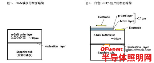
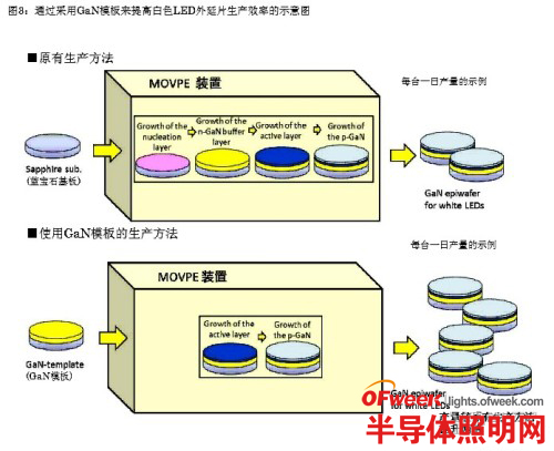
The gallium nitride template enhances LED characteristics. OFweek Semiconductor Lighting Network Hitachi Cable Co., Ltd. announced the successful development of a new mass production technology for the GaN template (Fig. 1) of high-quality gallium nitride (GaN) single crystal thin films grown on sapphire substrates, and has begun sales. By using this product as the underlying substrate of the " white led epitaxial wafer", the production efficiency of the white LED epitaxial wafer can be greatly improved, and the LED characteristics can be enhanced. Therefore, for the fiercely competitive white LED manufacturers, this product is expected to become a solution that can significantly enhance the competitive advantage of the company. In recent years, white LEDs have been rapidly expanding in the market for lighting products represented by liquid crystal panel backlights due to their significant advantages in energy saving and long life. The basic growth mode of the white LED epitaxial wafer is to first grow a 10 μm thick n-type GaN layer on the sapphire substrate, and then grow a 1 μm thick ultrathin active layer and p-type GaN layer (Fig. 2). In the general production process, these crystal layers are all grown by the MOVPE method (Note 1). Although the MOVPE method is suitable for the growth of an active layer requiring atomic-level film thickness control, it takes a long time to grow a high-quality n-type GaN layer of a desired thickness. Therefore, the white LED epitaxial wafer can only grow up to 1 or 2 times a day. Therefore, how to achieve high-efficiency production has always been a difficult problem to be solved in the industry. The GaN template employs a structure in which an n-type GaN layer is grown on a sapphire substrate. By using GaN stencils, LED manufacturers will no longer need the growth process of n-type GaN buffer layers, and the time required for growth will be reduced to about half. In addition, the GaN template produced by Hitachi Cable can also achieve low resistance and high crystallinity at the same time, which is also suitable for high-power LEDs that require large currents. Previously, Hitachi Cable has developed a single crystal GaN self-supporting substrate for devices such as blue-violet lasers, and in order to realize the production of this product, the development of unique crystal growth technology based on the HVPE (Note 2) method has been advanced. This time, based on this unique growth technology, we have developed a high-efficiency production technology and equipment for high-quality GaN templates, and built a complete mass production system. GaN templates mainly have the following characteristics: In addition to the previously developed GaN substrates and GaN epitaxial wafers, Hitachi Cable has introduced GaN stencil products, and will further strengthen and expand the GaN product lineup to provide compound semiconductor materials that can meet a wide range of customer needs. At the same time, Hitachi Cable will participate in the CS Mantech (International Conference on Compound Semiconductor Manufacturing Technology) held in New Orleans, USA from May 13 to 16, and will showcase the GaN template at the exhibition. Disposable Vape Pen,Latest Vape Pen,E Cigarette Fruit Flavor Disposable Longhua Manxueling Trading Company , https://www.mxlvape.com
In order to solve this problem, Hitachi Cable has developed a GaN template used for the underlying substrate grown by the MOVPE method.
(1) High crystallinity and high surface quality are achieved based on the growth technique accumulated during the development of the GaN self-supporting substrate;
(2) A low-resistance n-type GaN buffer layer suitable for high-power wafer-bonded LEDs and the like (Note 3;
(3) Support sapphire substrate with flat surface and various PSS (Note 4);
(4) Support for 2 to 6 inch diameter wafers (development of 8-inch wafers is under planning). 