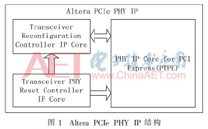
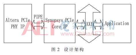
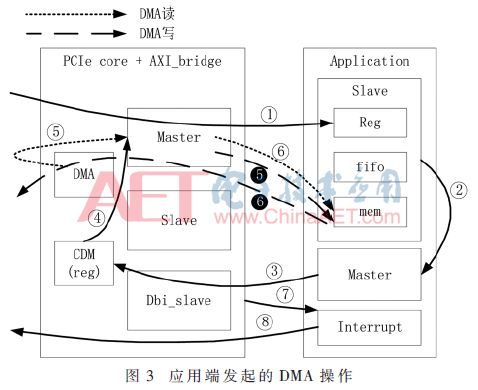
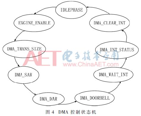
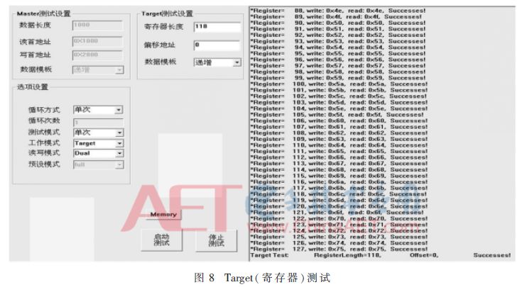
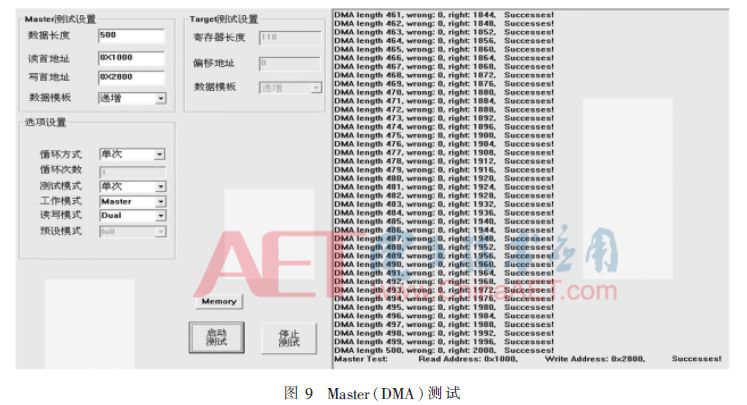
With the continuous development of communication technologies, the requirements for the speed and data transmission quality of data transmission systems are also increasing. The third-generation I/O bus technology proposed by Intel in 2001, PCI Express bus technology, uses high-speed differential serial data transmission for high-bandwidth, high-reliability, high-expansion, etc. Make up for the lack of PCI and PCI-X bus. Based on the PCIe 2.0 protocol, this paper proposes a DMA controller using Altera Transceiver PHY IP, Synopsys PCIe Core IP and AXI bus, and builds a high-speed data transmission system between the FPGA and PC. The register read and write operations (single word read and write) and DMA read and write operations are realized, and the system simulation and PC software in the Synopsys VIP environment are used to observe and verify the correctness of data reading and writing. 1.1 Basic module 1.1.1 Altera Stratix V GX Series FPGAs and PCIe PHY IP This design uses the 5SGXEA7K2F40C2N FPGA chip in the Stratix V GX family, which integrates the PCIe PHY IP hard core module. The PCIe PHY IP hard core consists of three parts, as shown in Figure 1. The PHY IP Core for PCI Express (PIPE) integrates the physical layer of the PCIe bus. The Transceiver Reconfiguration Controller IP Core dynamically reconfigures analog parameters. The Transceiver PHY Reset Controller IP Core acts as a reset module for the transceiver, ensuring initialization of the PCIe link. 1.1.2 Synopsys IP and VIP As the name suggests, VIP is Verification IP, which provides a standard bus behavior model for some standard interfaces. Synopsys provides the Controller IP of the PCIe bus, implements the data link layer and transaction layer functions of the PCIe bus, and has built-in DMA. It also provides a VIP for the PCIe bus and provides a standard bus behavior model for the PCIe bus. Simulated the function of the host computer [8]. 1.1.3 AXI bus AXI (Advanced eXtensible Interface) bus is a high-performance, high-bandwidth, low-latency bus protocol. It has a remarkable feature. The address/control and data channels are separated. There are five unidirectional channels, respectively read address channel. , write address channel, read data channel, write data channel, write response channel [9], reduce latency and improve the efficiency of DMA. 1.2 Overall plan design The overall architecture used in this design is shown in Figure 2. It is Altera PHY IP+Synopsys PCIe Core IP+AXI bus+Application. In order to take advantage of Synopsys' PCIe VIP environment, Synopsys PCIe Core IP is used. The AXI bus interface is used between the PCIe transaction layer and the application side, which can be easily extended and replaced in future designs. The application side design implements the function of the PCIe DMA controller and integrates two pieces of RAM, one block size is 128 DW, which is used to store data read and written by the register; the other block size is 512 DW, which is used to store data read and written by the DMA. 2.1 Application-side DMA operation flow The DMA operation flow initiated by the application side is shown in FIG. 3. The result of the final DMA read operation is that the data on the host side is written into the memory of the application side in a DMA manner. The result of the DMA write operation is to write the data of the application side to the memory on the host side in a DMA manner. FIG. 3 is a specific flow of the DMA operation initiated by the application end. (1) The host side writes the DMA read/write flag, DMA length, DMA source and destination memory address to the register of the application terminal by means of register writing; (2) The slave module in the application side sends these commands to the Master module; (3) The Master module transmits the commands to the internal registers of the PCIe Core IP according to the Synopsys PCIe Core IP customized Dbi bus. (4) The PCIe Core IP receives the DMA read/write command and continuously operates the Master interface to implement subsequent operations; (5) When reading for DMA, the built-in DMA of PCIe Core IP reads the target data from the "source memory address" on the host side; when writing for DMA, the master interface of PCIe Core IP is read by the AXI bus. Read from the "source memory address" to the target data; (6) When reading for DMA, the master of the PCIe Core IP obtains the target data read by the DMA, and writes it to the "destination memory address" of the application side through the AXI bus; when writing for the DMA, After the Master obtains the target data, the built-in DMA sends the data to the "destination memory address" on the host side; (7) When the DMA operation is completed, the PCIe Core IP notifies the interrupt module of the application; (8) The interrupt module on the application side will submit an interrupt to the host side. 2.2 Application side DMA control state machine The application only needs to write the DMA read/write flag, DMA length, DMA source and destination memory address and DMA start signal written by the host side to the internal registers in the PCIe Core IP, and wait for the completion of the DMA operation to give an interrupt signal. . The following is a detailed DMA control state machine for the application side. As shown in Figure 4, the state machine integrates the DMA read operation and the DMA write operation, reducing the amount of code. (1) IDLEPHASE: Idle state. When the start signal start_flag is valid, the ENGINE_ENABLE state is jumped; (2) ENGINE_ENABLE: Determine the DMA read/write type signal wr_rdn_flg. When wr_rdn_flg is 0, that is, DMA read (PC to FPGA), enable DMA read engine; when wr_rdn_flg is 1, it is DMA write (FPGA to PC) , enable DMA write engine; (3) DMA_TRANS_SIZE: set the DMA data transmission length, transfer 512 DW at most once, and transfer 1 DW at least once; (4) DMA_SAR: set the DMA operation source address (when the DMA is read, the source address is the host address; when writing for DMA, the source address is the application address); (5) DMA_DAR: Set the destination address of the DMA operation (when DMA is read, the destination address is the application address; when writing for DMA, the destination address is the host address); (6) DMA_DOORBELL: enable DMA operation doorbell signal dma_strt, start DMA operation; (7) DMA_WAIT_INT: waiting for the DMA operation to complete; (8) DMA_INT_STATUS: read the DMA operation interrupt register state, when the DMA operation completion signal dma_done is valid, a completion interrupt is generated, and the DMA_CLEAR_INT state is jumped; (9) DMA_CLEAR_INT: Clear the interrupt, return to the IDLEPHASE state, and prepare for the next DMA transfer. 3.1 Simulation verification After the code is written, the simulation platform is built in the VIP environment, and the function verification test is performed by Synopsys's simulation verification tool VCS. The main test verifies that the module can correctly correct the register read and write and DMA read and write. As can be seen from FIG. 5 and FIG. 6, the write address offset is 0x40, the write data is 32'h87654321, the read address offset is 0x40, and the read data is 32'h87654321, thereby judging that the register is correctly read and written. As shown in Figure 7, the dma_strt and dma_done signals can be seen as 2 DMA transfers. From dma_wr_rdn, the first time is DMA read operation (RC end to APP side), and the second time is DMA write operation (APP side). To the RC end, it can be seen from dma_bc_len that the current DMA operation length is 2 000 Bytes, that is, 500 DW, and the more dense parts of the slv_rdata and slv_wdata signals are the data of 2 DMA operations respectively. Comparing the two data, it is known that the DMA operation is correct. . In order to compare the results more conveniently, the method of automatically comparing files is to store the data written in the register or DMA into a file, and then store the data read back by the register or DMA into another file, by comparing the two files. The judgment register and DMA transfer are correct. 3.2 FPGA test verification After the simulation verification is completed, the FPGA test is verified. After the hardware part is burned to the FPGA chip of the board, the PCIe gold finger of the board is inserted into the motherboard of the PC, and the insertion of the PCIe hardware is detected after the PC restarts. The corresponding PCIe driver software can be installed and tested by the host computer. The upper computer software interface is shown in Figure 8, including register read and write (Target operation) and DMA read and write (Master operation) test module. Select the "dual" mode of the "Target" operation, the register length is set to 118, because the first 10 registers are related to DMA operations, may trigger DMA operations, so select Skip in the software. Click “Start Testâ€, the data will be written from the host side to the FPGA first, then read back from the FPGA to the host side, and compare the data of the two register operations to determine the correctness of the register operation. As shown in Figure 9, select the "dual" mode of the "Master" operation, click "memory", that is, open a memory on the PC side to store data, and then click "Start Test", the data is first written from the PC to the RAM of the FPGA. Then return to the PC from the FPGA, compare the data stored in the PC memory and the data written back to the PC from the FPGA, and then determine the correctness of the DMA read and write operations. According to the time when DMA transfers fixed-size data, the DMA read/write rate can be calculated. After multiple tests, the DMA read/write rates are 1 547 MB/s and 1 607 MB/s, respectively. This design uses PCIe Gen2, ×4 channels, and the theoretical maximum transfer rate is 2 000 MB/s. Analysis of the code may take a while because the application side writes and reads data to the PCIe Core IP. It takes some time for the driver to write or read parameters to the DMA register, which affects the rate. The DMA controller based on FPGA-based PCIe bus interface implemented in this paper is implemented on the basis of Altera PHY IP and Synopsys Core IP. The function simulation is verified by Synopsys VIP verification environment, and the system is measured by FPGA. The high transfer rate, in Gen2, ×4 mode, DMA read and write operations bandwidth of 1 547 MB ​​/ s and 1 607 MB / s, respectively, reached the expected design goals.
ZGAR MINI
ZGAR electronic cigarette uses high-tech R&D, food grade disposable pod device and high-quality raw material. All package designs are Original IP. Our designer team is from Hong Kong. We have very high requirements for product quality, flavors taste and packaging design. The E-liquid is imported, materials are food grade, and assembly plant is medical-grade dust-free workshops.
From production to packaging, the whole system of tracking, efficient and orderly process, achieving daily efficient output. We pay attention to the details of each process control. The first class dust-free production workshop has passed the GMP food and drug production standard certification, ensuring quality and safety. We choose the products with a traceability system, which can not only effectively track and trace all kinds of data, but also ensure good product quality.
We offer best price, high quality Vape Device, E-Cigarette Vape Pen, Disposable Device Vape,Vape Pen Atomizer, Electronic cigarette to all over the world.
Much Better Vaping Experience!
ZGAR Vape Pen,Disposable Device Vape Pen,UK ZGAR MINI Wholesale,ZGAR MINI Disposable E-Cigarette OEM Vape Pen,ODM/OEM electronic cigarette,ZGAR Mini Device Zgar International (M) SDN BHD , https://www.zgarecigarette.com