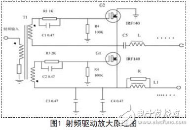
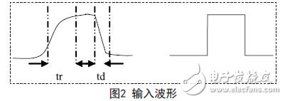
0 Preface As shown in Figure 1, the schematic diagram of the RF drive amplifier from the 1 kW PDM transmitter shows that the 0-+15V square wave pulse from the pre-excitation stage is input from the same name of the transformer T1 and is fed through the two secondary windings. The FETs G2 and G1 pick up the power, G2 and G1 push-pull the amplifier, and output a square wave pulse of 80V-100V. After the pre-selected frequency output of C5 and L, input to the last three power amplifiers. A brief analysis of the effects of various factors on the amplifier is given below. 1. Reasons for high frequency transformers The high-frequency transformer T1, the winding insulation paint is detached, or the winding is buried by the damp dust, causing a high-frequency short-circuit. The amplifier does not work because there is no input voltage, and there is no output voltage. Do not touch the high-frequency transformer easily during maintenance. Always remove the dust from the amplifier. If the insulation coating of the transformer winding is found to fall off, use insulating paint. 2. Effects of changes in parameters of capacitors C1 and C2 The FET is a voltage controlled device with high impedance at the input stage. It achieves energy conversion with high efficiency and low power consumption. The quality of the input stage voltage waveform has a significant impact on the amplifier. The ideal and actual waveforms of the IRF140 gate are shown in Figure 2. When an ideal square wave passes through the actual transmission channel, it is attenuated by "rolling off" and the erased shoulder forms noise. The effects of noise are not considered here. However, the rising and falling edges of the distortion have a great influence on the field effect tube, the waveform distortion is severe, the rising edge time is too long, the power loss of the amplifier is increased, the tube is heated, and the tube is thermally broken for a long time. The impact of the falling edge is the same. To do this, we need to correct the distortion of the input waveform. R1C1 and R3C2 are designed for this purpose. In actual maintenance, it is found that when C1 and C2 are used as mica capacitors or ceramic capacitors, the parameters are unstable, generally become smaller, and the correction of the opposite wave is worse, causing an unnamed burning tube. Here, the two capacitors are replaced with non-polar bile. This type of fault is eliminated after the capacitor. The purpose of correcting the waveform is to speed up the switching speed of the FET. 3.-72V DC voltage impact when switching on and off Although the filtering of C3 and C4 is suitable for the 70V DC voltage during the startup and shutdown, the interference pulse generated by the self-induction of L1 has a absorbing effect, but the effect is limited (because the value of C3, C4 cannot be too large, too large will affect the normal The path of the high-frequency carrier signal), especially when the FET is switched at a high frequency, forms a ringing interference at the shoulder of the output. For this reason, a 5W100K resistor R is connected in parallel across L1 to reduce the self-induced voltage. To eliminate adverse effects. Through the above replacement of some original parts of the amplifier and improvement of the line, the quality of the output waveform of the amplifier becomes better, the amplifier works stably, and the failure rate is significantly reduced. Air Glow Series Hongkong Onice Limited , https://www.osbvapepen.com