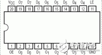
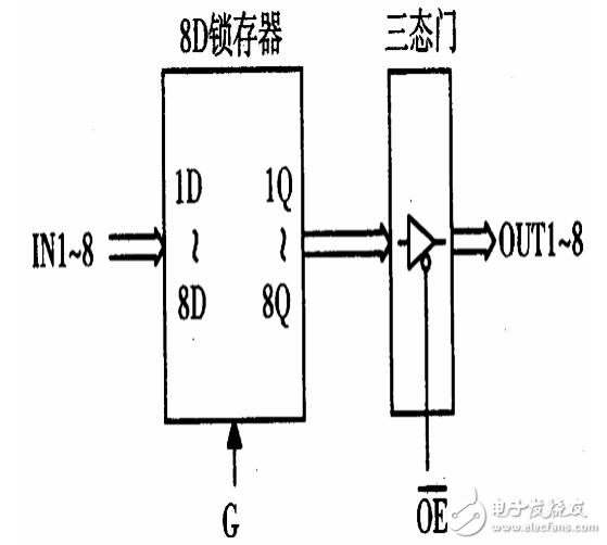
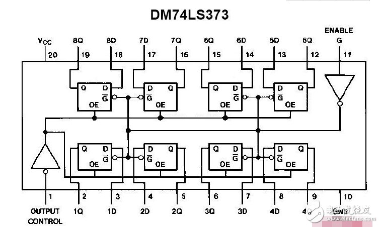
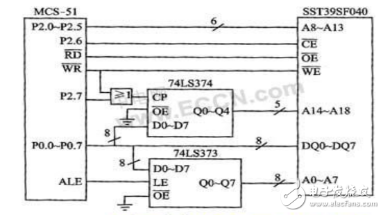
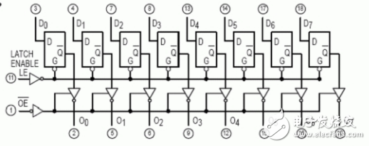
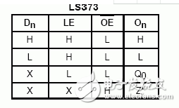
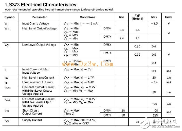
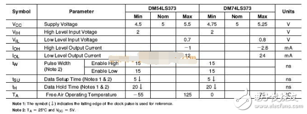
The 74LS373 is a commonly used address latch chip consisting of eight parallel D flip-flops with tri-state buffered outputs. In order to extend the external memory in a microcontroller system, a 74LS373 chip is usually required. This article describes how the 74LS373 works. G is the data entry end: When G is "1", the latch output state (1Q ~ 8Q) is the same as the input state (1D ~ 8D); when G changes from "1" to "0", the data is locked In the memory. (1).1 pin is output enable (OE), which is active low. When pin 1 is high, regardless of input 3, 4, 7, 8, 13, 14, 17, 18, no matter 11 How the pin (latch control terminal, G), output 2 (Q0), 5 (Q1), 6 (Q2), 9 (Q3), 12 (Q4), 15 (Q5), 16 (Q6), 19 (Q7 ) all exhibit a high-impedance state (or a floating state); (2). When pin 1 is low, as long as a falling edge appears on pin 11 (latch control terminal, G), output 2 (Q0), 5 (Q1), 6 (Q2), 9 (Q3), 12 (Q4) 15, 15 (Q5), 16 (Q6), and 19 (Q7) immediately present the states of the input pins 3, 4, 7, 8, 13, 14, 17, and 18. When the latch terminal LE goes from high to low, the 8-bit information at the output is latched until the LE terminal is valid again. When the tri-state gate enable signal OE is low, the tri-state gate is turned on, allowing Q0~Q7 output, and when OE is high, the output is left floating. When the 74LS373 is used as an address latch, OE should be made low. When the latch enable C is high, the output Q0~Q7 states are the same as the input terminals D1~D7; when C is negative During the transition, the input terminals D0~D7 are locked into Q0~Q7. The ALE signal of the 51 MCU can be directly connected to the C of the 74LS373. 74ls373 and microcontroller interface: 1D~8D is 8 inputs. 1Q~8Q is 8 outputs. G is the data latch control terminal; when G=1, the latch output is the same as the input; when G changes from "1" to "0", the data is input into the latch. OE is the output enable end; when OE=“0â€, the tri-state gate is open; when OE=“1â€, the tri-state gate is closed and the output is in a high-impedance state. In the MCS-51 microcontroller system, the 74LS373 is often used as an address latch. The connection method is shown in the figure above. The input terminals 1D~8D are connected to the P0 port of the single chip microcomputer, the output terminal provides the low 8-bit address, and the G terminal is connected to the address latch enable signal ALE of the single chip microcomputer. The output enable terminal OE is grounded, indicating that the output tri-state gate is always open 1, 74LS373 logic diagram 2, 74ls373 truth table 1, 74LS373 electrical parameters 2, 74ls373 recommended working conditions Our company specializes in the production and sales of all kinds of terminals, copper terminals, nose wire ears, cold pressed terminals, copper joints, but also according to customer requirements for customization and production, our raw materials are produced and sold by ourselves, we have their own raw materials processing plant, high purity T2 copper, quality and quantity, come to me to order it! Copper Connecting Terminals,Cable Lugs Insulated Cord End Terminals,Pvc Insulated Cord End Terminal,Cable Connector Insulated Cord End Terminal Taixing Longyi Terminals Co.,Ltd. , https://www.longyiterminals.com