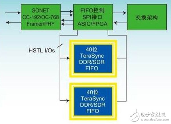
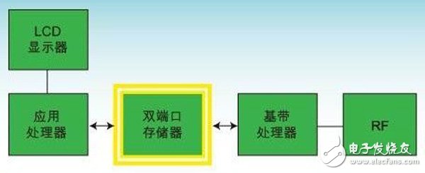
Many young engineers first think of programmable logic when considering potential design options at work. However, the increasing reliance on programmable logic has also led to problems that have often been overlooked in teaching circuit design, which has led many young engineers to create systems without realizing that there are many alternative technologies available to solve them. The design challenge. In many cases, the lack of knowledge in this industry choice is related to the lack of experience in setting up practices. The lack of expertise directly affects their ability to design high-performance, low-cost products. Figure 1: 40Gbps solution for high performance routers The best example of this trend of embedded buffer memory is the embedded data buffer storage application. For many years, FIFO and multiport memory have been the de facto standard for experienced design engineers to create cost-effective data buffer subsystems. However, as FPGA memory density increases, design engineers have chosen to use on-chip memory instead of discrete FIFO or multi-port memory. For advanced systems, it makes sense to integrate discrete FIFO or multiport memory functions into the FPGA. Integrating multiple data buffers and data control functions into one chip provides an even better solution. The appeal is to enable design engineers to reduce component count and minimize board space requirements. To help design engineers, FPGA vendors offer a set of standardized design building blocks to speed up the development process. However, good solutions require a certain amount of cost, and high-density FPGAs are not cheap. When the data bus speed exceeds 100MHz and a higher density buffer is needed, it is more expensive. Performance can also be a problem. Some performance limitations are not obvious when engineers integrate FIFO or multiport memory functions into programmable logic cells. In many cases, using discrete components or combining small FPGAs can provide a more ideal solution. The problem arises without consciousness. Given that educational institutions are overly reliant on programmable logic, many engineers today have lost awareness of the latest developments in discrete, dedicated memories, such as FIFOs and multiport memories. Semiconductor suppliers now offer FIFO devices with densities ranging up to 18Mb. The read and write ports are fully independent and operate at speeds up to 250MHz, and the DDR option enables up to 20Gbps per port performance. Numerous selectable port features allow the user to select the bus width, I/O voltage, data rate, and synchronous or asynchronous operation. The integrated flag operation (flag operaTIon) adds functionality to the device and, most importantly, pin compatibility across the entire product line makes it easy for design engineers to upgrade to higher densities and speeds. Multiport memory has a similar development process. Design engineers can choose between different bus widths per port and support devices between 8 and 72 bits. These devices operate at up to 200MHz in synchronous mode or 10ns in asynchronous mode with a density of up to 36Mb. Currently, the device can support a core voltage range of 5V, 3.3V, 2.5V or 1.8V. The I/O voltage is 5V, 3.3V, 2.5V, and 3.3V/2.5V or 1.8V can be selected. There are also a number of special features available, including full-boundary counters, independent byte enable, collision detection, interrupts, semaphores, and busy arbitration. Performance Limitations of Embedded Data Cache When engineers who have been educated using FPGAs design data buffer subsystems, they naturally prefer to design FIFOs as FPGAs. However, many people are unaware that the increase in the number of FIFOs in their designs exposes them to performance limitations. Typically, these engineers use tools from major vendors to automatically map multiple FIFOs into a single physical memory module, creating the logic needed for time domain multiplexing between multiple specific user FIFOs. However, because each individual FIFO port must be multiplexed together, the highest operating frequency of each FIFO port is inversely proportional to the number of FIFOs mapped into the design. Figure 2: Low-power dual-port devices are ideal for multimedia smartphones When each FIFO device operates independently with its clock, the total memory bandwidth between data, control inputs and status flags, and FIFOs is shared. When a read or write operation of a FIFO device is initiated, the sequencer circuit accesses the physical data in a fast Time Division Multiplexing (TDM) clock domain. The sequencer circuit then quickly accesses the physical memory of the TDM clock domain. The sequencer then passes the information back to the clock domain of the FIFO port to complete the memory access. Because of the transmission of the clock domain, the performance of the FIFO device is inherently limited by the speed of the sequencer circuit and the number of FIFOs used. In fact, some leading FPGA vendors recommend controlling the number of FIFOs in their devices to within 10 in high-performance designs. There are also a number of performance-related issues when configuring an FPGA as a dual port. In many of these applications, FPGAs are often tied to ASICs. Performance is controlled by three main factors: the intrinsic speed or the speed at which information is written and read from the dual port, the settling time or the time it takes for the ASIC input to become stable, and the speed at which the highest speed or external ASIC obtains dual port information. Sunset Lamp,Room Lights,Led Ceiling Lights,Kitchen Ceiling Lights Jiangmen soundrace electronics and technology co.,ltd. , https://www.soundracegroup.com
