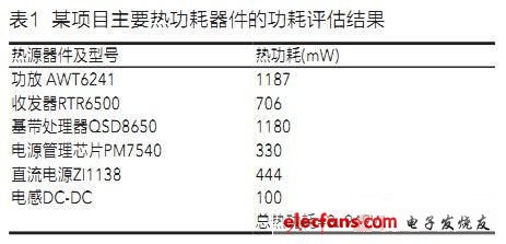
With the deployment of LTE wireless networks, the downlink data rate has reached and exceeded 1 Gbps. To handle such a high data rate, the data terminal must have high data processing capability and inevitably bring about an increase in power consumption. And some of the products we are developing have had hot problems. There are several prototypes that have crashed even in a few minutes during large-speed data transmission. The root cause of these problems is heat, and thermal design has become a problem. A challenge for card terminals. An example of Apple's iPAD product, a large number of users feedback that their products have problems in a higher environment, which reflects the importance of thermal design for end products. Power consumption has become a key issue for engineers to seriously consider in the early stages of product design. The heat source devices of the terminal platform mainly include baseband chips, radio frequency chips, power amplifiers, power management chips, etc. The power consumption of these devices can be found in the datasheet given by the manufacturer, and some can not be found, which cannot be found from the datasheet. The heat source device of the power consumption data needs to be estimated based on the test data of experience or similar projects, and the relevant data can be obtained directly from the platform provider. Table 1 shows the power consumption evaluation results of the main thermal power devices of a project. From the data in Table 1, we can see that the power consumption of a data card is close to 4W. In order to dissipate such a large amount of heat in the U disk-sized structural components, the thermal design of the PCB can be said to have become a product. A critical design consideration for reliable work. A thermal layout algorithm for card terminal products The empirical value of the heat flux density of natural convection cooling is 0.8 mW/mm2, that is, when the power distributed over the area per square millimeter is 0.8 mW, a good natural convection cooling effect can be produced. The calculation of the thermal distance of the heat source device is based on this empirical value. The calculation method is as follows: Let the length of a chip be L (mm) and the width be W (mm), and the power consumption of the device is Pd (mW). To achieve natural convection cooling, the PCB area that the device should occupy is: The thermal distance between the long side and the wide side of the device is equal, both of which are x (mm). The thermal distance is taken into account. The PCB area occupied by the device is: The above calculation only considers the single-sided heat dissipation of the PCB. The actual PCB can be cooled on both sides. If the other components are not placed on the back of the heat source device, the copper skin on the back side can also play a heat dissipation role. The thermal distance at this time will be calculated above. Half of the data, the PCB area occupied by the heat source device is calculated below. In the PCB layout, the above calculation data is often not feasible, because the PCB area is limited, if the layout according to the above data, the PCB area is not enough, so you need to compress the above data in a certain proportion, you can Dividing the above thermal distance by 2 as the thermal distance after compression, and thus calculating the compression heat distance, the PCB area occupied by the heat source device is as follows: Heated Seat Cushion,Portable Heated Seat Cushions,Heated Car Seat Cushion,Heated Seat Cushion Rechargeable Ningbo Sinco Industrial & Trading Co., Ltd. , https://www.newsinco.com
![]()
