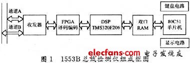
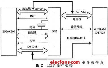
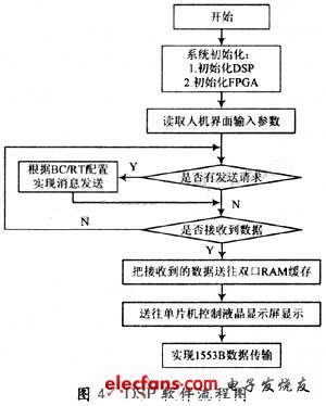
The MIL-STD-1553B bus protocol has developed into an internationally recognized data bus standard, which is widely used in avionics integrated systems. At present, most of the various 1553B bus capture cards developed at home and abroad use BU produced by the US DDC company. 6150 interface chip, but the price of this chip is relatively expensive, the development cost is relatively high, and many other merchants are thrilled. The design of the 1553B bus communication module based on DSP introduced in this paper uses TI's TMS320F206DSP chip for digital signal processing and FPGA for on-site repeated programming, which reduces the design cost and meets the development needs of the 1553B communication module. 1 Introduction to TMS320F206 The DSP of the 1553B bus communication module uses TI's TMS320F206, which is used to realize the main part of the 1553B bus protocol and realize the functions of word and message processing. TMS320F206 is a fixed-point DSP chip with high cost performance introduced by TI in recent years. Manufactured using static CMOS integrated circuit technology. The advanced Harvard structure of the DSP chip allows the program memory and data memory to be addressed and accessed independently. The two buses allow data and instructions to be read at the same time, thereby increasing the data throughput rate. Doubled; dedicated instruction set provides powerful signal processing operations. The main features of TMS320F206 are as follows: (1) 5V operating voltage, 20MHz main frequency, instruction cycle 50ns; 3 external pin interrupts; 8-level internal hardware stack, store call / interrupt return address; hardware wait; sleep IDLE mode, low power consumption; standard IEEE1149.1 simulation port. (2) On-chip 64k program space, 64k data space, 64kI / O space, 32k global storage space, on-chip 544 & TImes; 16b dual-addressable RAM, 32k × 16b user programmable FLASH, as program space, 4k × 16b single seek Address RAM, program space and data space can be moved before. (3) On-chip 16b timer, on-chip soft wait generator, which can generate 0-7 waits for program space, data space, and I / O space respectively. On-chip oscillator and phase-locked loop have frequency multiplication and frequency division functions. 32b arithmetic logic unit / accumulator, 16 × 16b multiplier, full-duplex asynchronous serial port UART, enhanced synchronous serial port, with 4-level FIFO. 2 Block diagram and working principle of the system The detector adopts single-chip technology, programmable logic device (FPGA) technology, digital signal processing (DSP) technology, combined with 1553B bus transceiver technology. It can not only perform offline detection of a single avionics device, but also perform online detection of the operation of the entire bus of the aircraft and the data transmission of various recording devices. The detector as a whole uses personal digital assistant (PDA) technology, data input, output, processing, control, display, etc. are all concentrated in the detector. The block diagram of the system composition is shown in Figure 1. From the aspect of data signal flow: when receiving data, the external data is sent to the transceiver for voltage conversion, and becomes a set of 20b serial data, which is processed into 16b parallel data by the FPGA chip EP20K200 and sent to the DSP for processing through the expansion port, and then through the double The RAM of the port is used for data buffering. When the data needs to be displayed, the single-chip CPU analyzes and stores the 16b parallel data sent from the dual-port RAM, converts it into hexadecimal, binary or engineering unit system according to the requirements and sends it to the display for display. When sending data, the CPU The data input by the keyboard is converted to hexadecimal, binary or engineering unit system, and then sent to the dual-port RAM buffer. The DSP reads the data from the dual-port RAM, pre-processes it and sends it to EP20K200, EP20K200 for conversion processing, and outputs a group of 20b The serial data to the transceiver is coupled into a serial data that meets the requirements of the 1553B standard through the transformer, and then sent to the data bus through the transceiver interface. 3 hardware circuit design 3.1 Receiver and transmitter In the 1553B avionics system, the coupling method is adopted between each terminal device and the bus, which is divided into transformer coupling and direct coupling. The BU-63152 chip of the American DDC company is used, with two completely independent dual redundancy ports. It fully meets the requirements of 1553B bus receiving and sending. In the receiver operation mode, under the control of pin STROMB, the data is changed to a bidirectional TTL level, which is output from the RX DATA OUT and its non-pin to the next stage decoding circuit. In the operation mode of the transmitter, under the control of the INHIBIT pin, the transmitter part receives data from the encoding circuit and sends it to the data bus. 3.2 FPGA module The combination of FPGA technology and digital signal processing DSP technology is a common method in modern electronic design. The FPGA chip interface in this module mainly implements the following functions: (1) Convert the serial information stream on the bus into parallel information that the processor can process or vice versa; (2) When receiving or sending information, it can identify or generate standard 1553B information words and messages. (3) Complete the information exchange with the processor, including the allocation of the 1553B information address, the decoding of the command word (or status word) or the return of the status word, and the sending data word. Using FPGA to realize the codec, its basic function is similar to the aforementioned BU-61580 chip, which is the key technology of the 1553B bus detector. 3.3 DSP module TMS320F206 is a fixed-point DSP with the lowest design cost and low structural complexity introduced by TI in recent years. On-chip 32k FLASH and 4.5k RAM can meet the task of moderate processing scale. The design of the DSP module in this tester is mainly To grasp the interface technology of clock circuit, interruption and data and address bus, the main interface circuit is shown in Figure 2. It can be seen from the DSP interface circuit diagram that the DSP module provides the clock circuit for the entire system. The interruption of the DSP chip is generated by EP20K200. On the one hand, it informs F206 to read the data, on the other hand, it notifies the DSP to perform error handling. Due to the pipeline operation mode of the DSP chip, Digital signal processing speed is powerful and meets the characteristics of 1553B protocol transmission rate. 3.4 Dual-port RAM and display module Because it is easy to cause data jamming in high-speed data processing and acquisition systems, the design of the high-speed data interface plays an important role in the smooth flow of data transmission throughout the system. The 8k dual-port static RAM IDT7025 used by DDC in the United States is used in this design. The problem of data jams. In this design, the display module adopts a hardware connection mode in which the memory is connected to the display module. The DSP sends the data to be displayed to the dual-port RAM. The 51 single-chip computer continuously scans the memory, makes corresponding processing according to the data in the memory, and constantly refreshes the content on the display. The BUSY signal line of the dual-port RAM is to avoid the left and right ports simultaneously. Hardware support is provided for write operations to the same storage unit. In the design, the liquid crystal display module uses a 16 × 16 dot matrix Chinese display module. 4 System software design The software design of the 1553B avionics bus detector mainly includes three parts, which are used to drive the data acquisition board, complete the configuration of each register, and realize the data transmission and reception detection. 4.1 FPGA control program This part uses the hardware description language VHDL for programming, synplify for synthesis, and Max + Plus II for timing simulation. The Manchester code encoder and decoder in the MIL-STD-1553B bus interface implemented on the FPGA can be implemented by the state machine. , Can be divided into 4 states; the first state line is the idle state, when the data transition edge is detected, enter the second state; the second state is the effective synchronization prefix detection state; when effective synchronization is detected At the beginning of the prefix, the third state is started, the clock is separated by a phase-locked loop, and the code conversion is performed; when the data is valid, the fourth state is entered for parallel / serial conversion and parity check. FPGA receives the data flow as shown in Figure 3. 4.2 DSP module control program The DSP part of the software uses C language and assembly language mixed programming, that is, it has the characteristics of strong portability of C language, and has the characteristics of fast execution speed and intuitive assembly language. In this design, the DSP software design mainly completes the communication between FPGA and its internal Register initialization; the operation of control commands when sending data to FPGA, the processing of command words when receiving data, the processing of status words, and notifying FPGA to accept data, etc., is the core part of the entire system control. Figure 4 shows the DSP software control flow chart. 5 Conclusion The avionics detector based on the 1553B bus is mainly used for online and offline detection of military avionics equipment, and meets the functions of BC and RT. The design of PDA also provides great convenience for detection. Of course, because the design is in the prototype stage, there are still some For the imperfect areas, there is still much room for improvement in the future. Street Lighting Poles,Street Lamp Post,Street Light Post,Street Lamp Pole Jiangsu Baojuhe Science and Technology Co.,Ltd. , https://www.galvanizedsteelpole.com
MIL-STD-1553B is a time-division, command / response, centralized control multiplexed half-duplex serial data bus. Its transmission speed is 1Mb / s, word length is 20b, data effective length is 16b, and information The maximum length is 32 words. The information format includes bus controller BC (Bus Controller) to remote terminal RT (Remote Terminal), RT to RC, RT to RT, broadcast type and system control type. 


Design of 1553B Bus Communication Detector Based on DSP
Design of 1553B Bus Communication Detector Based on DSP
Zhu Mingjun 1, Zhu Jun 1, Li Lun 2
(1. Air Force Engineering University, Xi’an, Shaanxi 710077, 2. People ’s Liberation Army 95430, Chengdu, Sichuan 610081, China)
This article is excerpted from the "electronic query network"