Lu Guimeng, a writer from the Tang dynasty, wrote in his golden poem “Gold is precious since ancient times, and still magnanimous and talentedâ€. This sentence was still not outdated even more than 1,000 years later. Because of its unique natural properties, gold is not only a special currency for reserves and investment, but also a “dominant†of the jewellery industry, even in the special industries such as the electronics industry, modern communications, and aerospace industry. material.
In the field of electronic design, perhaps for some audio enthusiasts' engineers, the application of gold in electronic products probably starts with the audio signal “lossless†transmission of high-fidelity top-matched gold-plated audio cables. More engineers learned from media reports that the chips were used to refine gold. In fact, there is no shortage of such “golden chips†around us. The RF MEMS switch released by ADI has once again brought the excellent metal properties of gold into full play. Let’s take a look at the excels of these gold-made chips.
 Mystery gold structure creates revolutionary switching performanceADI announced two revolutionary RF MEMS switches, the ADGM1004 0Hz to 13GHz MEMS switch with integrated driver, and the DC to 14GHz single-pole, four-throw MEMS switch ADGM1304 with integrated driver. The key advantage of MEMS switches is that it achieves 0 Hz/dc precision performance, wideband RF performance, and much better reliability than relays in a very small surface-mount package. In addition, the inherent “anti-day†performance of this series of MEMS switch designs is as follows:

Precision dc performance: Precision performance of < 2Ω RON, 0.5nA shutdown leakage current, -110dBc total harmonic distortion (THD + N), and the ability to fully improve performance levels through beam and substrate optimization.
Linearity performance: When the input signal tone is 27dBm, the third-order intercept point (IP3) exceeds 69dBm. There is potential for improvement above 75 dBm in all operating bands.
Lifetime: Guaranteed at least 1 billion cycles of action, which far exceeds any mechanical relays on the market today, which is typically rated at less than 10 million cycles.
Power handling (RF/dc): Over 40dBm of power has been tested across all operating frequency bands, with no degradation in performance at lower or higher frequencies. For DC signals, the switching technology allows more than 200mA to pass.
These features are undoubtedly excellent, and this is why MEMS switches have been regarded as excellent alternatives to limited-performance electromechanical relays for the past 30 years — because they are easy to use, small in size, and reliably reliable with minimal losses. Transmitting 0Hz/dc to hundreds of GHz signals has the opportunity to revolutionize the way electronic systems are implemented. However, due to the limitations of the traditional process, this kind of good performance can only be an imagination, and the ADI's launch of these two chips for the first time truly realized the commercial application. What plays a key role in this is the MEMS cantilever switch beam made from gold.

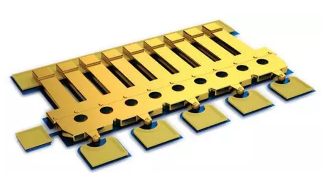
Figure 1: Key components in MEMS switch chips - gold-plated MEMS cantilever switch beams.
Engineers accustomed to circuit design may not be accustomed to the internal structure of the MEMS chip. In fact, each MEMS device has a large number of mechanical structural components. The photo above shows a microscopic view of a gold cantilever arm structure that is privately known by the ADI engineers as the "gold finger." Only a tiny 6-micron structure has 5 fingers (contacts), and this is what the switching device can become The key to revolutionary products in the industry, ADI invested a lot of money in research and development of gold plating technology, and built these highly consistent products with specialized MEMS production lines.
The “gold finger†uses electrostatic action to apply a high voltage DC voltage under the cantilever beam to control the conduction of the switch. When on, the electrostatic attraction pulls cantilever down and all 5 contacts are lowered. The on-resistance of each contact is 5 ohms. After the combination, the overall on-resistance will be much smaller, allowing for greater Power passed. After testing, the "gold finger" transmission power can reach 36dBm.
The cantilever beam is made of gold, but the gold-to-gold contact design is not conducive to improving the operating life, so the contact material is changed to carbide metal, so its service life - that is, the number of switches has been greatly improved. The actual moving distance when the “gold finger†is turned on is only 0.3 micrometers. The tiny moving distance and the ADI patented sealed case technology all contribute to the improvement of reliability. Reliability is the key to mechanical design. MEMS relay products composed of four groups of 'gold fingers' can achieve a switching life of one billion times. In terms of number of movements alone, this is regarded as the most revolutionary breakthrough in the field of switching!
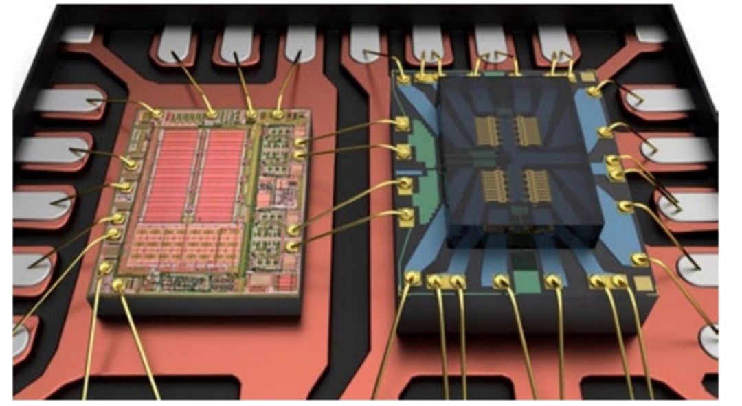
The lead pad is also connected to a metal lead frame using gold wire bonding and then packaged into a plastic quad flat no lead (QFN) package for easy surface mounting on the PCB. Chips are not limited to any kind of packaging technology. This is because a high-resistivity silicon cap is soldered to the MEMS die, forming an airtight protective case around the MEMS switching device. Regardless of the external packaging technology used, this airtight enclosure improves the environmental robustness and service life of the switch.

Figure 2: The driver IC (left) and the MEMS switch chip (right) are mounted and wire bonded to the metal lead frame.
Alloys made of gold material undergo "phallic-like tests" at high temperatures
The above switch products make good use of the good electrical conductivity of gold. In fact, gold's excellent physicochemical properties include extremely high resistance to chemical corrosion and discoloration, and no melting or oxidation at temperatures of up to 1000 degrees Celsius. , no discoloration, no loss, and its high temperature resistance also obtained many applications in electronic products.
Many applications require signal processing solutions that can operate at temperatures above 125°C, but the maximum operating temperature for standard-design integrated circuits is typically only 125°C. Whether it is to steer an oil rig at ground and ground or perform precision measurements on jet engines, it needs to operate at near-extreme temperature, and therefore requires specialized solutions to ensure performance and reliability. For these demanding applications, ADI offers products specifically designed for extreme temperatures that are certified to operate at temperatures from 175°C to 210°C, and are particularly suitable for oil and gas exploration, geothermal monitoring, and industrial engines. Control and other applications.
In fact, if such integrated circuits are exposed to extreme temperatures, their performance and reliability are often reduced by many factors. For example, an increase in substrate leakage current in an exponential manner and changes in device parameters with temperature can result in a performance penalty. Packaging-level issues such as wafer level issues such as electromigration and wire bond wear can also compromise reliability. To overcome these challenges, ADI's high temperature product line has been specifically designed using innovative silicon processes, packaging and test techniques, and is certified to work in high temperature environments.
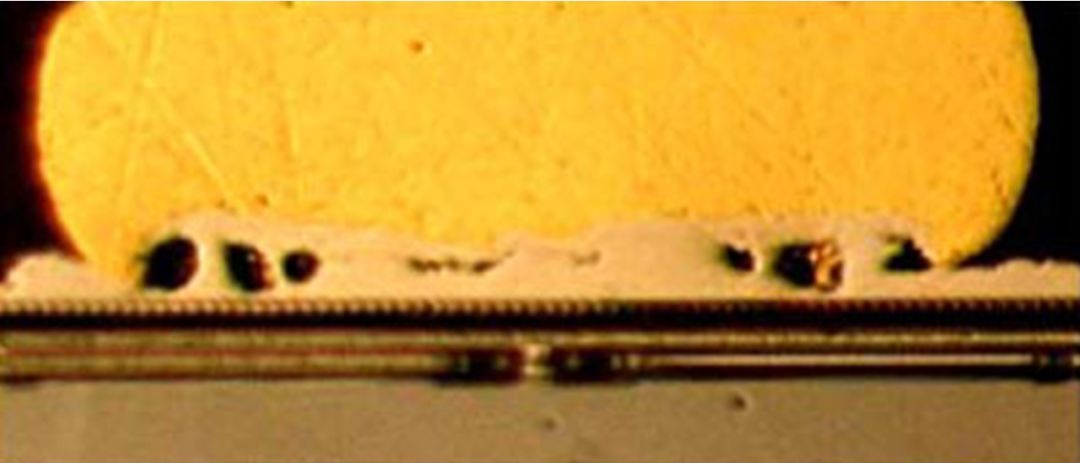
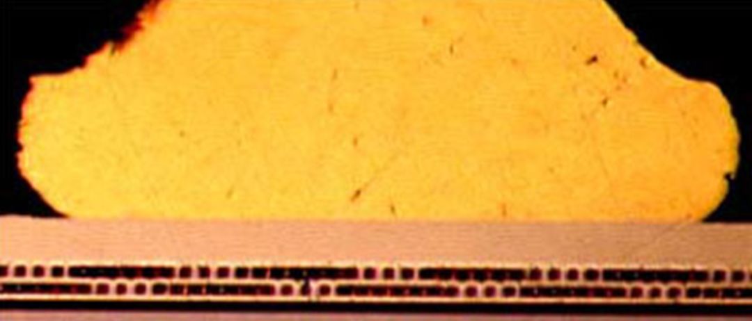
Among them, the process based on gold materials has played an important role. ADI's wire bonding process for HT plastic packaging is another main technology to ensure package reliability in high temperature environments. Ordinary gold/aluminum wire bonds will degrade with increasing temperature, forming void-containing fragile intermetallic compounds that weaken the weld strength. The entire process may take only a few hundred hours. ADI added a nickel-palladium-gold metallization process to the HT plastic package to obtain a gold pad surface, which is then used together with the gold wire to achieve a delicate metal weld that avoids the formation of intermetallic compounds. The graph below shows the reliability gains achieved using this technology – in high temperature environments, after 500 hours standard gold/aluminum solder joints will show significant voids and form intermetallic compounds while the right side uses nickel-palladium-gold metal Welding of the process remains intact after more than 6,000 hours.

Figure 3: Gold/Aluminum wire welding after 500 hours at 195°C.

Figure 4: Nickel-palladium-gold isolated gold/gold wire welds after 6,000 hours at 195°C.
ADI's HT product process flow includes a comprehensive reliability certification program tailored to the needs of high temperature applications. All HT products meet the high temperature operating life (HTOL) test of the JEDEC JESD22-A108 specification. Each product has at least three batches that require a minimum of 1000 hours of testing at the highest temperature to ensure compliance with the data sheet specifications. Products based on this type of process technology are also familiar to the engineering industry in the industry, including the ADXL206 accelerometer, the ADXRS645 gyro, the AD8229 instrumentation amplifier, and the ADG798 multiplexers, as well as the ADG5298.
USB 2.0 Hub
Another version of USB HUB.When comparing 2.0 and 3.0 there are a few major differences. First the transfer rates: USB 2.0 offers transfer rates of 480 Mbps and USB 3.0 offers transfer rates of 4.8 Gbps - that's 10 times faster. Note that the transfer speeds also depend on the device in use in addition to the bus type and USB ports and cables.

USB 2.0 Hub,Macbook Usb Hub,Macbook Pro Hub,Hub for Laptop
Pogo Technology International Ltd , http://www.wisesir.net