Implementation of RF digital short-wave transmitter frequency conversion module and AD conversion module program tutorial
Firstly, the basic principle of the RF digital short-wave transmitter and the main functions of the AD9957 chip are briefly introduced. Then, a scheme of using the Q99C mode of the AD9957 chip to implement the internal digital up-conversion module and the digital-to-analog conversion module of the RF digitized short-wave transmitter is proposed. In this mode, the methods of baseband data generation, clock configuration and serial port programming are elaborated. Finally, the simulation results and hardware measurement results of the application scheme of AD9957 in short-wave transmitter are given.
1 IntroductionThe design of the digital short-wave transmitter is to make the digital to analog converter (DAC) close to the antenna as much as possible, and replace the traditional analog signal processing with digital signal processing whenever possible. With the improvement of hardware levels such as DSP and FPGA, RF digital short-wave transmitters have become a reality. This paper introduces a dedicated chip that can perform orthogonal up-conversion and digital-to-analog conversion, AD9957, and analyzes the application of AD9957 in RF digital short-wave transmitter.
2. Principle of RF digital shortwave transmitterEarly short-wave transmitters are analog systems. The audio input signal is SSB modulated, multi-mixed, filtered and amplified, and the audio signal can be moved to the RF band. In the RF digitized short-wave transmitter, most of the analog circuits are replaced by digital circuits. The baseband signals are directly forwarded by the digital up-conversion module to the short-wave transmission band; the DAC completes the conversion of the digital signals to the analog signals; the analog signals pass through the power amplifier and the matching network. Finally, it is transmitted by the antenna [1], as shown in Figure 1.

The AD9957 chip is a general-purpose digital quadrature upconverter from Analog Devices. It integrates a high-speed, direct digital synthesizer (DDS), a high-performance, high-speed 14-bit DAC, clock multiplier circuit, and digital Filters and other DSP functions [2]. The AD9957 has three modes of operation: Quadrature Digital Up Converter (QDUC) mode, DAC interpolation mode, and tone mode. Using the QDUC mode of the AD9957, digital up-conversion and digital-to-analog conversion in the RF digitized short-wave transmitter can be realized.
In QDUC mode, two orthogonal signals are input: I(t) and Q(t), and the data distributor and formatter deinterlace I and Q so that each sample runs along the internal data path in parallel. transmission. The half-band filter and the Cascad Comb Intergrator (CCI) filter interpolate the baseband signal to increase the sampling rate of the input signal by 4 times and 2 to 63 times, respectively. Increasing the baseband signal sampling rate is the ability to multiply and add to the quadrature (sine and cosine) local oscillator signals generated by the DDS core to produce a quadrature upconverted data stream. The inverse CCI filter and the inverse SINC filter compensate for the passband amplitude attenuation produced by the CCI filter and the DAC, respectively. The functional block diagram of QDUC mode [3] is shown in Figure 2.
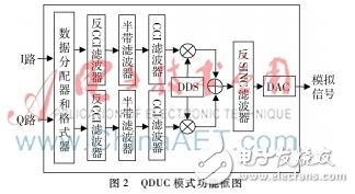
/4.1I/Q data generation
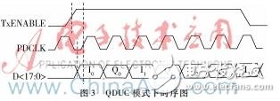
The I/Q data is the in-phase component and the quadrature component of the baseband data, respectively, and the size of each sample point is represented by 18-bit twos complement or offset binary. The capacity of the baseband data is determined by the combination of the data duration and the sampling rate. For example, to send 1 s baseband data at a sampling rate of 5 MHz, 1 & TImes; 5 & TImes; 18 = 90 Mbit data capacity is required. If the baseband data is a rectangular pulse train, it must be pulse shaped before entering the chip data port. The data read timing diagram in QDUC mode is shown in Figure 3. TxENABLE is a signal that strobes user data and allows data to be latched into the device when the signal is true. PDCLK is a parallel data clock that is equal to the sampling rate of the baseband data. Normally, the rising edge of PDCLK is used to latch data to the data port. In QDUC mode, the I and Q data words alternate on the parallel port of the AD9957, and each PDCLK active edge captures an 18-bit I or Q word. Therefore, the PDCLK clock rate is:

Where fSYSCLK is the sampling rate of the DAC; R is the interpolation factor of the CCI filter. The half-band filter interpolation factor is fixed value 4, and the CCI filter interpolation factor is R. The rate of each of the I or Q data is fSYSCLK/4R, so the PDCLK clock rate is fSYSCLK/2R.
4.2 clock configuration
There are two ways to provide the reference clock input to the AD9957 through the REF_CLK/REF_CLK input pins on the chip, which are direct drive and crystal drive.
Direct drive allows direct input of signals between 60 MHz and 1 GHz as the system clock for the chip. It is also possible to input a low frequency signal that is multiplied by a phase-locked loop (PLL) inside the chip to 400 MHz to 1 GHz. The crystal drive generates a reference clock from the crystal and then multiplies it to the corresponding system clock band.
AD9957 adopts a digital-analog hybrid phase-locked loop, namely Charge Pump Phase-Lock Loop (CPPLL). Its basic structure is shown in Figure 4. It is mainly composed of Phase Frequency Detector (PFD). Charge pump CP (Charge Pump), low-pass filter LPF (Low-Pass Filter), frequency divider (Divider) and voltage controlled oscillator VCO (Voltage Control Oscillator) composed [4].
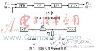
The LPF uses a third-order loop filter [5], as shown in Figure 5.
Figure 5 third-order passive loop filter
R2 is 1 kΩ and C3 is 1.1 pF. The rest of the parameters are welded on the periphery of the chip according to the design requirements. The calculation formula is as follows:
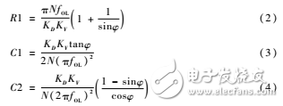
Where KD is the charge pump current value; KV is the VCO gain; N is the feedback distribution coefficient; φ is the phase margin; fOL is the open loop bandwidth.
In the hardware test, take KD = 287 μA, KV = 500 MHz / V, N = 20, fOL = 1.2 MHz, φ = 45 °. It is calculated that R1 is 1 211 Ω, C1 is 300 pF, and C2 is 46 pF.
4.3 serial programming
The AD9957 serial I/O port is compatible with most synchronous transport formats including the Motorola 6905/11 SPI and Intel 8051 SSR protocols [2].
The serial communication cycle can be divided into two phases. The first is the instruction phase, which writes the register address byte to be accessed to the AD9957 and defines the second stage for writing or reading. The second phase is a write cycle or a read cycle, which refers to transferring data from the serial port controller to the serial port buffer and reading data from the valid registers, respectively. At the end of the write cycle, the programming data resides in the serial port buffer and is in an inactive state. I/O_UPDATE transfers the data in the serial port buffer to a valid register. For the read cycle, I/O_UPDATE is not required and data is output on the falling edge of the clock.
In addition, the AD9957 supports MSB first or LSB first transfer formats. The serial interface port can be configured as single-pin input/output (SDIO) or dual-pin input and output (SDIP and SDO); I/O reset (I/O_RESET) signal and active-low chip select (CS) signal control Whether serial communication is carried out improves the flexibility of the design system.
5 ConclusionA custom sequence (1011010) with a bit rate of 2 kb/s is used as the baseband data, and the QDUC mode function circuit is built by Systemview software, and the simulation is verified. In the simulation process, the raised cosine filter used in pulse shaping has a roll-off factor of 0.5, 200 times interpolation filtering, and the output carrier frequency is 25 MHz. The simulation results are shown in Fig. 6.
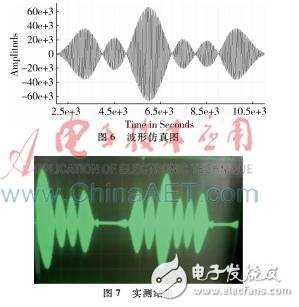
The hardware test results are shown in Figure 7. The actual test results are basically consistent with the simulation results.
In summary, the AD9957 is applied to short-wave transmitters to achieve RF digitization, which is practically feasible.
Generator Spare Parts,Diesel Engine Part,Rectangular Flat Key Parts,Engine Cylinder Head Parts
Jinan Guohua Green Power Equipment Co.,Ltd. , https://www.guohuagenerator.com