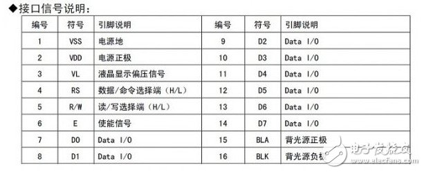
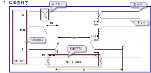
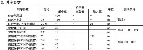
Operational timing is always the most important content of any IC chip. All usage details for a chip are included in its official device manual. So the first thing to do well with a device is to extract and grasp the useful contents of its device manual. Current China's chip design capabilities are limited, so most of the devices are manufactured by foreign IC giants such as TI, AT, and MAXIM. The device data is naturally also in English, so the foundation of English is to read these. The data sheet was improved. Even if there is a Chinese translation, it is advisable to read the original English version. If you do not understand it, you may wish to refer to the Chinese version again. This will help you to improve. Let's first look at the 1602 pin definition. The 1602 pin is a neat SIP single inline package, so the device manual only shows the pin's functional data table: We only need to pay attention to the following pins: 3 pin: VL, LCD bias signal, used to adjust the LCD1602's display contrast. External potentiometer is generally used to adjust the bias signal. Note that this pin's voltage is 0 can get the strongest contrast. 4 feet: RS, data / order to choose the end, when this foot is high level, can carry on the transmission operation of the data byte to 1602, and when it is level, it is the transmission operation of order byte. The command byte, which is the byte used to set some of the operating modes of the LCD 1602; the data byte, even if used to display the byte on 1602. It is worth mentioning that the LCD1602 data is 8-bit. 5 feet: R/W, reading and writing choose end. When this pin is high, data can be read from the LCD1602, otherwise data can be written. The author believes that this pin is not very practical, and permanently grounding it permanently will not affect its normal operation. However, this has not been verified by complex systems. 6 feet: E, enable signal, it is the data control clock signal of LCD1602 actually, use this signal rising edge to realize the data transmission to LCD1602. 7~14 feet: 8-bit parallel data port, making reading and writing of LCD1602 much easier. Now look at the operating sequence of the LCD1602: Here, we can not read the status of its data or the data itself. So only need to look at two write timings: 1 When we want to write the instruction word, set the working mode of LCD1602: RS needs to be set to low level, RW is set to low level, then the data is sent to data port D0~D7, and the last E pin has a high pulse. Write data. 2 When we want to write the data word, when the display is implemented on the 1602: RS needs to be set high, RW is set to low, then the data is sent to the data port D0 ~ D7, and finally a high pulse on the E pin Write data. Discovered, write instructions and write data, the only difference is that the level of RS is not the same. The following is the timing diagram of LCD1602: Now look at the operating sequence of the LCD1602: Here, we can not read the status of its data or the data itself. So only need to look at two write timings: 1 When we want to write the instruction word, set the working mode of LCD1602: RS needs to be set to low level, RW is set to low level, then the data is sent to data port D0~D7, and the last E pin has a high pulse. Write data. 2 When we want to write the data word, when the display is implemented on the 1602: RS needs to be set high, RW is set to low, then the data is sent to the data port D0 ~ D7, and finally a high pulse on the E pin Write data. Discovered, write instructions and write data, the only difference is that the level of RS is not the same. The following is the timing diagram of LCD1602: We must slowly learn to look at the timing diagram. We must know that the essence of operating a device is hidden in it. To understand the timing, you control this chip is very easy. The 1602 timing is one of the simplest timings I have ever seen: 1. Pay attention to the timeline. If it is not indicated (actually, most of them are also not marked), then the direction from left to right is the time forward axis, ie the time is increasing. 2. The above diagram outlines and illustrates some of the common sense of reading this diagram: (1). The leftmost of the timing diagram is generally a pin identifier, indicating that this row diagram reflects the change of the pin. The figure above shows the timing changes of the four types of pins: RS, R/W, E, and DB0~DB7. (2). The cross-lined portion indicates that the level is changing, as noted above. (3). It should be relatively easy to understand, as shown in the upper right corner of the above figure, the two parallel lines correspond to high and low levels, which also coincides with the statement of (2) medium level change. (4). Below the figure, the sealed diamond part, pay attention to the seal, indicating that the data is valid, the word Valid Data also shows this. 3. It is important to note that the level changes of the various pins in the timing diagram are based on the same time axis. Be sure to observe the timing diagram precisely in strict accordance with the growth direction of the time axis. Make the device strictly follow the timing diagram changes. This requirement is particularly stringent for single-bus devices such as 18B20. 4. The above points are not specific to the timing diagram of LCD1602. Most of the timing diagrams follow such general rules. Therefore, everyone must be accustomed to such rules slowly. Maybe you also noticed that there are many times marked on the time. This is also a very important information. The time stamps indicate the shortest or longest time for certain states to be maintained. Because the operating speed of the device is also limited, it is generally unable to keep up with the speed of the main control chip, so they have timing cooperation between them directly. Now that the frequency of various processors is growing wildly, it is not necessarily a dream to have a dual-core microcontroller in the future. The following is the timing parameter table: We must understand how to estimate the instruction time of the master chip. We can find some MCU parameters in the official data sheet. For example, we now use the AVR M16 as the main control chip, the external 12MHz crystal oscillator, the instruction cycle is a clock cycle (1/12MHz) us, so at least determine the time it executes a command is us level. We see that the time parameters given above are all ns level, so even if we do not add a delay program in the program, we should be able to well meet the timing requirements of the LCD1602. How to look at this table? Very simple, we can find in the timing diagram TR1, corresponding to the timing parameter table, you can find this is the E rising / falling edge time, the maximum is 25ns, that the level changes on the E pin, must be in the maximum 25ns The time within is completed. Does everyone mean this? Now I will interpret my understanding of this sequence diagram: When the command byte is to be written, the time changes from left to right, RS goes low, and R/W goes to low level. Note that the state of the RS changes first. Then, at this point, the data on DB0~DB7 goes into the active phase, and then there is a full-pulse transition on the E pin, and then the E pulse width whose minimum value is tpw=400ns is maintained. Then the E pin changes negatively, the RS level changes, and the R/W level changes. This is a complete LCD1602 write command sequence. Portable Power Station 2000W,Electrical Power Station,Portable Emergency Power Station,Portable Solar Charging Station Guangdong pisen electronics co., ltd , https://www.pisenpro.com


