There are currently hundreds of books on signal integrity and noise reduction in the market. If you are a newbie or need a refresher course, you might consider reading "Signal Integrity Issues and PCB Design" by Douglas Brooks. For a more in-depth discussion, read "High Speed ​​Digital Design" by Howard Johnson.
When you are going camping, on your way to RV travel, adventure, sailing, or cruising on your boat, a power supply is critical to satisfying the need for some electronic appliances. Although traditional lead acid batteries dominate a large market of outdoor power supply, lithium ion batteries are growing popular between outdoor adventures and travelers. Choosing LiFePO4 batteries over lead-acid batteries for any application can bring you numerous benefits, you can enjoy a faster charging time, a lower self-discharge of batteries, easier maintenance, longer lifespan of lithium batteries and much more.
The UFO Lithium Battery Packs include the popular sizes used in the lead-acid batteries but with the advantages of LiFePO4 technology. It maintains a ideal performance for deep cycle applications. At the heart of each UFO RV Lithium batteries is UFO PCM to take control of the battery performance and prevent the batteries from potential failure.
Solar Lithium Ion Battery,Rechargeable Lithium Battery,Rechargeable Li Ion Battery,Lifep04 Battery Pack,Home Storage Battery,Solar Lifepo4 Battery
Rv Battery,Rv Lithium Battery,Li Ion Battery Rechargeable,Rv Battery 12Volt ShenZhen UFO Power Technology Co., Ltd. , https://www.ufobattery.com
FPGAs can cause severe damage to signals (or other FPGA signals) in the system due to too much high-speed SSO, as this can lead to noise called simultaneous switching noise (SSN). SSN is also called ground bounce or VCC bounce. For single-ended standards, SSN is to provide transient currents from low to high and transient currents from high to low. Simultaneous switching and results from multiple output drivers. The change between the device voltage and the system voltage.
When the high-to-low transition causes a ground bounce, the low-to-high transition can also cause VCC to drop. Since the capacitor is usually placed between VCC and the ground plane, SSN typically exists in these two places. The rebound from low to high may also occur. As a result, SSO becomes an interfering signal, which produces noise that may be coupled to adjacent signals. Too much SSO for a region can cause power disturbances. For the following two reasons, SSO has become a problem that must be taken seriously: 1. The switching time is drastically reduced; 2. The reduction of via size and trace width plus the larger board thickness has pushed up the board inductance. This will greatly increase the likelihood of a rebound. Larger load capacitance may also cause SSN, though to a lesser extent. SSN can also cause timing problems to become prominent when the effective VCC is below the expected value, causing the I/O cache to switch below the desired speed.
There are several ways to reduce the SSN. Some devices simply simplify this issue by limiting the choice of I/O standards, but not all devices can do this. Some vendors recommend distributing high-speed bus outputs over the entire die. If the SSN is your only concern, then this is definitely a good suggestion. However, if you follow this recommendation, there are two basic issues that will arise. 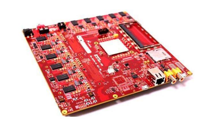
First of all, this may cause downstream layout problems, because spreading the signal across the entire die often causes more trace crossings. This leads to the need for more signal wiring layers. Second, most designs also require careful investigation before spreading the signal, as block/interval compatibility problems arise when a bus is spread out to a specific block or area. Therefore, if you can carefully distribute a small bus to one or two blocks/areas while considering the generality of the layout, then the system will work well.
If you are plagued by a design with adjacent high-speed switching outputs, there are several techniques that can help you solve potential SSN problems. First lay out and decouple your design. For decoupling, use power and ground plane pairs as close as possible, separated by an SMT capacitor. Decoupling using SMT capacitors also helps reduce inductance, which is a major factor in generating system noise.
If you still feel that you need to use decoupling capacitors (to reduce the SSN), you should place these capacitors as close to the high-speed output pins as possible. A study by Altera found that if these capacitors are more than 1 inch apart from the pins, these capacitors become inefficient when decoupled with appropriate SMT capacitors. Other suggestions to reduce the SSN or its possible impact include: Avoid placing sensitive signals (reset, clock, and enable, etc.) near SSO; use smaller offset outputs and use the lowest inductance vias when possible; The insertion delay at the appropriate position causes the output signal to alternate. Even if PCB production has been completed, this proposal can still be applied.
Refer to the related information of the device to be connected to the FPGA. For each device, determine the maximum input low voltage threshold (in millivolts). This is the maximum voltage that the FPGA needs to drive the device, so the device can still detect a valid logic low state (maximum VIL value). Also, determine the maximum input negative pulse signal (in millivolts) that the device can tolerate and continue to operate.
In some cases, the maximum allowable ground bounce may not be or not only the values ​​given above. Instead, the maximum system ground bounce is determined by obtaining the minimum value of the maximum input low voltage threshold, the maximum input negative pulse signal, or the maximum ground bounce of all devices.
Then, similar FPGA buses are grouped according to the number and kind of network connections with similar load characteristics. It then examines the number of power and ground pins for each section, region, or block, and the number of SSOs allowed for each power and ground pin pair for each I/O standard used. These numbers can be used to calculate the total capacitive load of each group and the capacitance of each output driver to determine the maximum SSO that can be tolerated.
You should also consult the supplier to determine if you exceed the recommended number of SSOs on a per-block and per-pair basis, provided that the supplier has studied these issues. At the same time, because there are multiple factors that lead to SSN, it is best to build a robust system with built-in noise immunity. Otherwise, use the device that limits the I/O standard for each pin, so that possible SSN problems can be reduced.
Differential Communications In FPGA design, you may find that the processing of differential signals is the most controversial. Similar to SSN, it is best to get as much information as possible from suppliers, books, and user groups. In the meantime, consult with your layout department to find out about the recommendations and information they recommend before deciding on a solution.
The main debate begins with whether differential signal pairs should be broadside or edge coupled and how much coupling should exist between each pair. The answer is usually "determined on a case-by-case basis," so a specific study is required.
If you can't determine why you need to choose differential I/O standards for a single-ended signal, the answer is simple. Using differential signals, you can almost completely control the loop of the signal. Because this is part of the signal pair, and theoretically no current from the signal pair should appear on any ground (or power) plane.
It is assumed here that the trace pairs have equal lengths, are arranged in adjacent areas and the spacing does not change, and the trace impedances are constant and matched. In addition, with single-ended signals, it is difficult for you to control the signal backhaul, and testing the return of a signal may also be futile.
The main disadvantage of differential signals is that they require two traces to be close to each other. This can be a difficult point when distributing hundreds of differential signals on one PCB.
-- Deep depth of discharge. Lithium batteries are designed to last longer with a deep depth of discharge. It enables some electronics such as high-tech and smart devices to work for a longer time.
-- Fast charging speed. When using lithium batteries for your electronic device, you can save time for charging and improve working efficiency.
-- Long service life. The lithium batteries provides up to 2000 cycle life with proper use. The features of less maintenance and longevity makes it a perfect option for power supply.
-- Wide temperature range. The lithium batteries can withstand extreme temperature. It can work in a cold winter or hot environment without battery failure. It is suitable for outdoor applications.