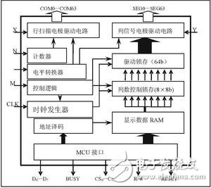
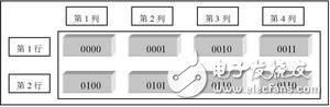
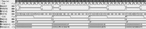
introduction LCD has many advantages such as low operating voltage, low power consumption, large display information, long life, easy integration, easy portability and low electromagnetic radiation pollution. It has been widely used in display technology and is widely used in mobile phones, PDA products and handheld instruments. In portable electronic products and equipment such as meters. The LCD driver circuit is an important component of the liquid crystal display system. It is an interface circuit between a computer (or MCU) and a liquid crystal screen. Its main function is to modulate the phase and peak value of the potential signal outputted to the electrodes of the liquid crystal display device. Parameters such as frequency are used to establish an AC drive electric field. Due to the large difference in the specifications of LCDs, the conventional method is to develop a dedicated driving circuit for each type of LCD, which is a waste of time and has poor reusability. To this end, designing an IP core that can be used in most small-scale LCD driver circuits is necessary to solve this problem by multiplexing the IP core. At present, only Yu-Jung Huang of I-Shou University and others have designed the IP core of the driver circuit that can drive LCDs of different sizes, and this function is realized by embedding an embedded microprocessor in the system. However, such embedded microprocessors make the system more complex and costly. The IP core of the driver circuit designed to drive different scale LCDs is realized by FPGA, which can effectively overcome the two disadvantages of complicated circuit system and high cost. Figure 1 IP core system structure Figure 2 IP core cascade diagram Figure 3 row control function simulation results Figure 4 column control function simulation results Design specification In order to meet the practical needs of most of today's smaller LCD display applications, the LCD driver circuit IP core chip designed in this paper has 64 COM (row) and 64 SEG (column) outputs, and has a high-speed 8-bit parallel MCU interface. And the serial interface, the chip contains RAM for storing display data, and specially designed 10 control terminals, which can be conveniently and flexibly controlled. It mainly has the following main functions: 1. Providing scanning timing signals and display signal data for the liquid crystal display; 2, support directly connected to the MCU in the form of a bus; 3, can drive LCD (n & TImes; m) of different scales, n can take values ​​continuously (n = 0 ~ 63), m can only take multiples of 8 (m = 8k, k takes natural numbers); 4. Support cascading between IP cores to drive larger-scale LCDs, supporting up to four IP inter-line cascades and inter-column cascades; 5, can provide a wider range of drive output voltage to adapt to different LCD devices; 6, provide picture-in-picture, split screen display and other functions. IP core design In accordance with the "top-down" design method, this paper firstly divides the chip into hierarchical functions, and refers to the design experience of the existing LCD driver chip, and combines the "bottom-up" design method to design some modules. Finally, According to the system design framework, each module is coordinated, and the overall function verification of the chip is performed, thereby meeting the requirements of the design specification. system structure The structure of the IP core system designed in this paper is shown in Figure 1. The IP core is mainly composed of the following modules: row scan and column signal drive module, level shifter, presetable number ring counter, data latch module, control logic module, display data RAM and address decoding module, MCU Interface module. Some of the large modules can also be subdivided into several sub-modules. Module design MCU interface module The MCU interface module is an interface between the IP core and an external controller (MCU), and is a channel for data transmission. The MCU writes commands, read states, or display data to the LCD driver chip through the interface. At the same time, the interface also accepts the control of the command decoder, thus combining read and write with internal operations. The chip is realized by more complicated internal combination logic and sequential logic circuit, and can be compatible with the current two mainstream MCU control signals, and supports two serial/parallel data operation modes. In addition to several sub-modules commonly used in the MCU interface module of the existing common LCD driving circuit, such as a data bus (8-bit) sub-module, a busy state detecting sub-module, a read-write control sub-module, and an MCU release sub-module, A new row cascade and column cascade control submodule has been added. The data bus is mainly used for internal and external data exchange; the busy status detection sub-module is used to judge the MCU status, generate a system busy flag signal to coordinate the read/write operation of the signal and receive the internal/external reset signal; the read/write control sub-module is used to generate the correct The read/write control timing of the MCU; the function of the MCU release sub-module is to release the MCU when the chip performs the "read-modify-write" process, so that the MCU can perform other operations at the same time; and the newly added cascade control The main function of the module is to realize row cascading and column cascading between IP cores, up to 16 IP cascading (four levels in each row), CS0~CS1 are row cascading control terminals, and CS2~CS3 are column grading. Connected to the console. For example, suppose there is an LCD (128 & TImes; 256), which can be driven by 8 IP cores. When set, CS is 0000, 0001, 0010, 0011, 0100, 0101, 0110, 0111, which can constitute 2 & TImes; The IP core array is driven, and its arrangement diagram is shown in FIG. 2. Display data RAM and address decoding module The module is mainly used for storing data to be displayed, and functions as a buffer between the MCU interface and the signal driving circuit to ensure stable output of the display data. The module includes two sub-modules of a RAM array and an address decoder for storing display data. First, the column address circuit provides the column address, and the column address decoder selects a column of 8-bit RAM memory cells, and the MCU reads/writes it through the interface; then, the row address decoder scans the RAM in units of rows. In combination with the display data latch circuit, the output of the entire line of data can be realized, and outputted to the liquid crystal display through the electrode driving circuit for display. Data latch module The module contains two sub-modules: a column number control latch sub-module and a drive latch sub-module. The column number control latch sub-module is composed of k parallel 8-bit data latches. The main function is to latch the data on the data bus and output it from the RAM to the 8 under the control signal and clock signal of the control logic module. The display data signals on the bit data bus are respectively latched in the corresponding 8-bit data latches, and the 64-bit data needs to be 8 times, each time inputting 8 bits. The drive latch sub-module is a 64-bit drive latch formed by connecting 64 1-bit latches in parallel. Its function is to put the above 8 8-bit data under the control signal and clock signal of the control logic module. The m-bit data transmitted from the latch is latched all at once and then input to the subsequent column signal electrode driving module. Control logic module The main function of this module is to control the number of signal data transmissions and select column signal lines. The column number control latch sub-module, the drive latch sub-module, and the clock generator can be controlled by the column number control input terminal M to implement functions suitable for LCDs of different sizes. According to the need, by inputting different values ​​to the column number control input M, it is controlled how many column number control latches are in the working state, and the other latch units are set to the idle state. The data in the display data RAM is latched into the corresponding column number control latch through the 8-bit data bus during the duty cycle, and then latched into the drive latch next time under the control of one clock signal to serve as an electrode driver. The input signal of the module. In this way, the IP core can implement the function of controlling the number of selected drive columns. When M is "000", the lower 8 bits (first latch) of the column number control latch work, the other is fully idle, the corresponding column electrode is SEG0~SEG7; when M is "001" The lower 16 bits (first and second latches) of the column number control latch operate, the other are fully idle, the corresponding column electrodes are SEG0~SEG15; and so on, until the column number control latch 64 The bit registers all work, and the corresponding column electrodes are SEG0~SEG63. Electrode drive module The module mainly contains four sub-modules: a row scan electrode driving sub-module, a column signal electrode driving sub-module, a level shifter and a presetable number ring counter. The function of the level shifter is to convert the voltage of the logic signal into the actual LCD driving voltage through an external control signal according to the needs of the actual application, and output it to the driving module; the function of the row scanning electrode driving sub-module is to provide the row electrode The scanning signal pulse of a certain period; the function of the column signal electrode driving sub-module is to apply data from the latch to the corresponding column electrode, and establish a AC driving electric field with the scanning signal of the row electrode, thereby driving the display of the LCD device. The preset number ring counter can control the number of row scanning electrodes through the row number control terminal N (S0~S5) to adapt to different scales of the LCD screen, and input different values ​​to the row number control terminal N according to actual needs. Control the number of rows for a specific job, and all other electrodes are idle. Under the control of the row drive clock signal, the progressive scan is repeated, until the row number control terminal N inputs a new value, and then a cycle scan is performed on the new number of row electrodes. For example, when the applied signal N is "011011", the number of scan electrodes is 27, the row scan driving sub-module generates a progressive scan signal on the row electrodes COM0~COM26, and all the other row electrodes COM27~COM63 are set to a low level. The cycle is reciprocating. If a new applied signal N is applied to "100011", the scan electrode driving sub-module generates a cyclic progressive scan signal on the row electrodes COM0~COM34. IP core system implementation Firstly, according to the above definition and division of the whole system function and the design of each module, each functional module is modeled by VHDL language. Secondly, on the FPGA device of Xilinx, the EDA tool ISE is used for simulation and synthesis. Debug and optimize the design; then, use VHDL to define the top-level module to connect the modules, and perform corresponding system debugging and verification; finally, get an LCD driver circuit with 64 COM (row) and 64 SEG (column) Output, there is a high-speed 8-bit parallel MCU interface and serial interface, the chip contains RAM for storing display data, and can be cascaded to expand to meet the larger LCD through the cascade control terminal CS, through the column number control terminal M and line number control terminal N to adapt to LCDs of different sizes. Simulation and verification This paper uses Xilinx's simulation software ISE as a simulation tool to verify the designed IP core in two steps. First of all, this paper firstly carried out preliminary functional verification on each module of the IP core (including the internal submodules). Then, with reference to the working process of the chip, the entire chip was simulated. Figures 3 and 4 show the simulation results obtained by simulating the row and column control functions of the entire IP core using ISE. In the figure, CLK and CLK1 are the data transmission control clock and row electrode scan pulse of the MCU interface module respectively; M and N are the control terminals for the number of column electrodes and row electrodes respectively; the lower two bits and the upper two bits of CS are respectively line cascading Cascade control with columns. The simulation results in Figures 3 and 4 illustrate: 1. When RESET is high, the IP core is in the initial state or cleared state; when WRITE is high, the IP core is in the working state and can receive display data. 2. On the rising edge of the clock CLK, the MCU writes 8-bit display data in parallel to the RAM of the IP core through the interface; on the rising edge of the clock CLK1, the row scan driving electrode sequentially outputs the scan pulse, and the column signal electrode will put the data in the RAM. Output from the SEG. 3. The number of rows control can change the number of electrodes for row scanning. When the number of rows selection control terminal N is "3E", the scan signal is output at COM0~COM61. As shown in FIG. 3, in the first row clock signal, the scan signal is outputted on the electrode COM61, and the row electrode is scanned step by row under the row drive clock control; when the seventh row clock signal, N becomes " 22", the scan signal becomes output on the row electrode COM33, and the progressive scan of COM0~COM33 is performed line by line. 4. The number of columns can change the number of electrodes in the column signal. When the column number selection control terminal M is "110", the SEG electrode is a 48-bit output; when M is "010", the output of the SEG becomes 16 bits; when M is "101", the output of the SEG becomes 40 bits. When M is "100", the output of the SEG becomes 32 bits. In this paper, the functions of column number control, row number control, and inter-core cascade of the IP core are verified respectively and verified. The limitation of the number of columns and the number of rows is only described here. Conclusion This paper discusses the design of an LCD display driver chip IP core. According to the top-down design idea, the chip is hierarchically functionalized and the overall function of the chip is verified. In the function verification of the chip, this paper uses the VHDL hardware description language to verify the logic function and timing relationship of the circuit. The LCD display driver has a good portability due to its parametric design, and can be conveniently applied to various scale flat panel display system applications of portable instruments and PDAs and the like.
ZGAR Vape Disposable Pods
ZGAR electronic cigarette uses high-tech R&D, food grade disposable pod device and high-quality raw material. All package designs are Original IP. Our designer team is from Hong Kong. We have very high requirements for product quality, flavors taste and packaging design. The E-liquid is imported, materials are food grade, and assembly plant is medical-grade dust-free workshops.
From production to packaging, the whole system of tracking, efficient and orderly process, achieving daily efficient output. WEIKA pays attention to the details of each process control. The first class dust-free production workshop has passed the GMP food and drug production standard certification, ensuring quality and safety. We choose the products with a traceability system, which can not only effectively track and trace all kinds of data, but also ensure good product quality.
We offer best price, high quality Pods, Pods Touch Screen, Empty Pod System, Pod Vape, Disposable Pod device, E-cigar, Vape Pods to all over the world.
Much Better Vaping Experience!
ZGAR Neo Vape Pods, ZGAR Disposable Vape, ZGAR Vape Pods System Vape,ZGAR Vape Pods Disposable Pod Vape Systems Zgar International (M) SDN BHD , https://www.oemvape-pen.com